Showing posts with label Using. Show all posts

Wednesday, 15 March 2017

Adjustable Voltage Current Power Supply Circuit Using IC L200


IC2 is connected as a differential amplifier and compares the signals at its two inputs.
Referring to the circuit diagram: the input comprises a mains switch, fuse, transformer, bridge rectifier and smoothing capacitor (C2). 


The difference between the inputs is the voltage drop across 'current’ sensor R4. This IC feeds the current sensing input (pin 2) of the L200. 


P1 in the feedback loop of the 741 is used to vary the output current of the circuit. IC1 must be mounted on a suitable heat sink as it dissipates nearly all the power of the circuit.
The reference level output from I pin 4 of IC1 goes to the voltage divider made up of R5 and P2 (this pot sets the value of the output voltage).


The power supply can quite easily be built into a case and a voltmeter and ammeter mounted on the front panel. ln view of the accuracy of the circuit these should ideally be digital meters, but virtually any type will do.


If you compare the expense and the rating of this power supply you will get a surprise, because the output voltage and current are fully adjustable between O. . . 18 V and 0 . . . 1.8 A respectively and costs have still been kept very reasonable. 


Diode D5 and capacitor C1 produce a negative auxiliary voltage, which is stabilized by zener diode D6 and capacitor C4. 


All this is necessary to enable the output voltage to be adjusted down to zero volts. During the construction of this part of the circuit bear in mind that the positive lead of electrolytic capacitor C4 is connected to earth! Regulation is provided by IC1 and IC2. Capacitor C3 suppresses any residual transients at the input of lC1 and it should therefore be connected as closely as possible to IC1 similarly C4 and IC2). 


The negative voltage provides the negative supply for the two ICs.


 Adjustable Voltage, Current Power Supply Circuit Using IC L200

Readmore → Adjustable Voltage Current Power Supply Circuit Using IC L200

Saturday, 11 March 2017

Grid tied solar pv system using single inverter Centralized inverter


Readmore → Grid tied solar pv system using single inverter Centralized inverter

Thursday, 9 March 2017

Solar Lamp using the PR4403


The PR4403 is an enhanced cousin of the PR4402 40 mA LED driver. It has an extra input called LS which can be taken low to  turn the LED on. This makes it very easy  to build an automatic LED lamp using a  rechargeable battery and a solar module. The LS input is connected directly to the solar cell, which allows the module to be  used as a light sensor at the same time as  it charges the battery via a diode. When  darkness falls so does the voltage across  the solar module: when it is below a thresh-old value the PR4403 switches on. During  the day the battery is charged and, with  the LED off, the driver only draws 100 µA.
Circuit Diagram :
Solar Lamp-Circuit Diagram
Solar Lamp using the PR4403 Circuit Diagram

At night the energy stored in the battery is released into the LED. In contrast to similar designs, here we can make do with a single  1.2 V cell. The PR4403 is available in an SO-8 pack-age with a lead pitch of 1.27 mm. The  other components are a 1N4148 diode (or a Schottky 1N5819) and a 4.7 µH choke. Pin 2 is the LS enable input, connected directly to the solar module. According to the datasheet, it is possible to connect a series resistor at this point (typ. 1.2 M) to increase the effective threshold voltage. The LED will then turn on slightly earlier in the evening before it is not completely  dark. Pins 3 and 6 of the device must be connected together and together form the output of the circuit.

Readmore → Solar Lamp using the PR4403

Friday, 24 February 2017

Using IFR Voltage Regulator Circuit Diagram


The IFR EW a MOSFET transistor, such as transistor has higher feature high input impedance. In this circuit we used an IFR as transistor voltage regulator, which is not common, but it is very good to learn about their behavior in a circuit.

 Using IFR Voltage Regulator Circuit Diagram


Using IFR Voltage Regulator Circuit Diagram


This voltage regulator circuit uses a MOSFET is
IRF4905 (Vdss =-55V, RDS (on) = 0.02ohm, Id =-74A),
but any other can be tested.

Readmore → Using IFR Voltage Regulator Circuit Diagram

Thursday, 16 February 2017

Simple LED flasher circuit using NE555 timer IC


This circuit consumes more power, but it's advantage is when you need a variable flash rate, like for strobe circuits. You can actually use this circuit as a remote control for strobes that have a remote input. Of course, it has many other applications besides strobes.

Simple LED flasher circuit using NE555 timer ICLED flasher circuit
  • R1, R2, C1 and the supply voltage determine the flash rate. Using a regulated power supply will do much to insure a stable flash rate. For a variable flash rate, replace R1 with a 1 megohm pot in series with a 22k resistor.
  • The duty cycle of the circuit (the percentage of the time LED 1 is on to the time it is off during each cycle) is deterimed by the ratio of R1 to R2. If the value of R1 is low in relationship to R2, the duty cycle will be near 50 percent. If you use both LEDs, you will probably want a 50 percent duty cycle. On the other hand, if R2 is low compared to R1, the duty cycle will be less than 50 percent. This is useful to conserve battery life, or to produce a strobe type effect, when only LED1 is used.
  • The NE555 timer chip can be damaged by reverse polarity voltage being applied to it. You can make the circuit goof proof by placing a diode in series with one of the supply leads.
  • The purpose of R3 and R4 is to limit current through the LEDs to the maximum they can handle (usually 20 milliamps). You should select the value of these according to the supply voltage. 470 ohms works well with a supply voltage of 9-12 volts. You will need to reduce the value for lower supply voltages.
  • Rainbow Kits offers several kits to build the above circuit. You can also order these kits from RadioShack.com. The Radio Shack catalog numbers (and web pages) are as follows: standard kit with two 5mm red LEDs, (990-0067), kit with two red, two green and two yellow 3mm LEDs, (990-0063), kit with jumbo green LEDs, (990-0048), kit with jumbo red LEDs, (990-0049). You can also buy all the parts to build the circuit at your local Radio Shack store, including a circuit board (276-159B).
I have built a miniature strobe circuit as follows. Use a 250k pot in series with a 4.7k resistor for R1. The 4.7k resistor sets the upper flash rate limit. Use 2.2k for R2. That sets a really short duty cycle. For this circuit, you don't use LED 2 or R4. For LED 1, I used a two Radio Shack white LEDs in series and no R-3. The circuit runs on a 9 v battery.  link

Readmore → Simple LED flasher circuit using NE555 timer IC

Monday, 13 February 2017

Sine Wave Generation without ECCP Using single CCP Module of PIC16F877A


I had previously shown how to generate sinusoidal pulse width modulation (SPWM) signals using the ECCP module in a PIC for generating a sine wave output for use in DC-AC inverter. I have had requests from people asking how to generate the same SPWM signals with other microcontrollers that don't have the ECCP module, such as the super popular PIC16F877A.

So, here I talk about how to generate the same SPWM signals using just one CCP module as can be commonly found on so many microcontrollers. This allows much greater flexibility in microcontroller selection.

You should go through the other articles related to generating SPWM with the ECCP module (if you haven't already gone through them, that is) to get an idea of what I'm talking about regarding sine wave generation with the ECCP module and about sine wave generation in general, really:

  • Generation and Implementation of Sine Wave Table
  • Smart Sine - Software to generate sine table
  • Generation of sine wave using SPWM in PIC16F684
  • 600W 50Hz sine wave inverter test circuit
  • Feedback in sine wave inverter (PIC16F series based)
  • Demystifying The Use of Table Pointer in SPWM - Application in Sine Wave Inverter

The code I had previously used (utilizing the ECCP module) is:


//----------------------------------------------------------------------------------------
//Programmer: Syed Tahmid Mahbub
//Target Microcontroller: PIC16F684
//Compiler: mikroC PRO for PIC (Can easily port to any other compiler)
//-----------------------------------------------------------------------------------------


unsigned char sin_table[32]={0,25,49,73,96,118,137,
159,177,193,208,220,231,239,245,249,250,249,245,
239,231,220,208,193,177,159,137,118,96,73,49,25};


unsigned int TBL_POINTER_NEW, TBL_POINTER_OLD, TBL_POINTER_SHIFT, SET_FREQ;
unsigned int TBL_temp;
unsigned char DUTY_CYCLE;

void interrupt(){
     if (TMR2IF_bit == 1){
        TBL_POINTER_NEW = TBL_POINTER_OLD + SET_FREQ;
        if (TBL_POINTER_NEW < TBL_POINTER_OLD){
           CCP1CON.P1M1 = ~CCP1CON.P1M1; //Reverse direction of full-bridge
        }
        TBL_POINTER_SHIFT = TBL_POINTER_NEW >> 11;
        DUTY_CYCLE = TBL_POINTER_SHIFT;
        CCPR1L = sin_table[DUTY_CYCLE];
        TBL_POINTER_OLD = TBL_POINTER_NEW;
        TMR2IF_bit = 0;
     }
}

void main() {
     SET_FREQ = 410;
     TBL_POINTER_SHIFT = 0;
     TBL_POINTER_NEW = 0;
     TBL_POINTER_OLD = 0;
     DUTY_CYCLE = 0;
     ANSEL = 0; //Disable ADC
     CMCON0 = 7; //Disable Comparator
     PR2 = 249;
     TRISC = 0x3F;
     CCP1CON = 0x4C;
     TMR2IF_bit = 0;
     T2CON = 4; //TMR2 on, prescaler and postscaler 1:1
     while (TMR2IF_bit == 0);
     TMR2IF_bit = 0;
     TRISC = 0;
     TMR2IE_bit = 1;
     GIE_bit = 1;
     PEIE_bit = 1;
    
     while(1);
}
//-------------------------------------------------------------------------------------


That's the previous code. Now let's look at the code based on a single CCP module and not the ECCP module. For this, I chose the super popular PIC16F877A microcontroller. The chosen frequency, like before, is 16kHz. The code is:
 

//----------------------------------------------------------------------------------------
//Programmer: Syed Tahmid Mahbub
//Target Microcontroller: PIC16F877A
//Compiler: mikroC PRO for PIC (Can easily port to any other compiler)
//-----------------------------------------------------------------------------------------


unsigned char sin_table[32]={0, 25, 50, 75, 99, 121, 143, 163, 181,
198, 212, 224, 234, 242, 247, 250, 250, 247, 242, 234, 224, 212, 198,
181, 163, 143, 121, 99, 75, 50, 25,0};


unsigned int TBL_POINTER_NEW, TBL_POINTER_OLD, TBL_POINTER_SHIFT, SET_FREQ;
unsigned int TBL_temp;
unsigned char DUTY_CYCLE;

sbit MOSA at RD0_bit;
sbit MOSB at RD1_bit;
sbit MOSC at RD2_bit;
sbit MOSD at RD3_bit;

unsigned char FlagReg;
sbit Direction at FlagReg.B0;
//0 -> MOS A + D
//1 -> MOS B + C

void interrupt(){
     if (TMR2IF_bit == 1){
        TBL_POINTER_NEW = TBL_POINTER_OLD + SET_FREQ;
        if (TBL_POINTER_NEW < TBL_POINTER_OLD){
           //CCP1CON.P1M1 = ~CCP1CON.P1M1; //Reverse direction of full-bridge
           if (Direction == 0){
              MOSA = 0;
              MOSD = 0;
              MOSB = 1;
              MOSC = 1;
              Direction = 1;
           }
           else{
                MOSB = 0;
                MOSC = 0;
                MOSA = 1;
                MOSD = 1;
                Direction = 0;
           }
        }
        TBL_POINTER_SHIFT = TBL_POINTER_NEW >> 11;
        DUTY_CYCLE = TBL_POINTER_SHIFT;
        CCPR1L = sin_table[DUTY_CYCLE];
        TBL_POINTER_OLD = TBL_POINTER_NEW;
        TMR2IF_bit = 0;
     }
}

void main() {
     SET_FREQ = 410;
     PORTD = 0;
     TRISD = 0;
     PR2 = 249; // 16kHz
     CCPR1L = 0;
     CCP1CON = 12; //PWM mode
     TRISC = 0xFF;
     TMR2IF_bit = 0;
     T2CON = 0x04; //TMR2 on
     while (TMR2IF_bit == 0);
     TMR2IF_bit = 0; //Clear TMR2IF
     PORTC = 0;
     TRISC = 0;
     TMR2IE_bit = 1;
     GIE_bit = 1;
     PEIE_bit = 1;
    
     while (1);
    
}


Now let's talk about the changes I've made in order to be able to use a single CCP module instead of the ECCP module.

When the ECCP module is used, it generates the SPWM signals and sends the modulation signals to the required "MOSFETs" (of course there's a drive circuit in between) depending on the "direction" as dictated by CCP1CON.P1M1 (bit 7 of CCP1CON register). Since this bit does not exist in the CCP module (obviously, since it's "uni-directional"), this functionality must be achieved in software. Since we don't have the ECCP module and have chosen to use a single CCP module only, the 4 drive signals come from other pins not associated to the PWM module. I've chosen PORTD bits 0 to 3. Of course, you can select any other 4 pins.

This is the circuit diagram of the SPWM signal generation portion:


Fig. 1 - Circuit diagram of SPWM generation section - microcontroller + AND gates (Click image to enlarge)

Below (Fig. 2) is the circuit diagram for the configuration of the MOSFETs and the drivers - and the synchronization with the signals generated from Fig. 1 above.


Fig. 2 - MOSFET Configuration Section (Click image to enlarge)

The SPWM generation is done by the single CCP module and which MOSFETs to send the signals to is set by the "Direction" bit and the hardware trick employing the AND gate. When "Direction" is equal to 0, the high side MOSFET A is kept on for 10ms during which time the SPWM signals on CCP1 output (RC2) are sent to low side MOSFET D by sending a "1" to RD3, which, with the help of the AND gate "diverts" the CCP1 signal to the low side MOSFET D (see Fig. 1 above). The same thing is achieved when "Direction" is equal to 1, just with high side MOSFET C and low side MOSFET B. When MOSFETs A and D are operated, MOSFETs B and C are kept off and vice versa. The MOSFETs are first turned off before the other two are turned on, as can be seen in the code block:

           if (Direction == 0){
              MOSA = 0;
              MOSD = 0;
              MOSB = 1;
              MOSC = 1;
              Direction = 1;
           }
           else{
                MOSB = 0;
                MOSC = 0;
                MOSA = 1;
                MOSD = 1;
                Direction = 0;
           }


To understand how the timing and the table pointer operation work, go through this:

Demystifying The Use of Table Pointer in SPWM - Application in Sine Wave Inverter

I've modified the sine table to increase the deadtime. Notice how there's a 0 at both the start and the end. This achieves the additional deadtime. See Fig. 4 below. I did this by using my software "Smart Sine" to generate a sine table with 31 values and then adding a 0 at the end.
 
Besides that, the other functionality are the same - the PWM initialization and setting, the table and table pointer are used the same way as before. So make sure you go through this tutorial if you aren't completely clear regarding it:

Demystifying The Use of Table Pointer in SPWM - Application in Sine Wave Inverter

For the MOSFET drivers, you require high/low side MOSFET drivers. One of the most popular such driver is the IR2110. For a thorough tutorial on using the IR2110, go through this tutorial:
http://www.blogspot.com/2016/01/using-high-low-side-driver-ir2110-with.html

Here are the simulation results:


 Fig. 3 - Generated SPWM  Drive Signals (Click image to enlarge)


Fig. 4 - Clear demonstration of the "deadtime" (Click image to enlarge)


Fig. 5 - Simulation results showing signal frequencies (Click image to enlarge)


Fig. 6 - Generated Sine Wave Signal (Click image to enlarge)


The operation is quite simple to understand. The trick lies in a simple software modification and the use of the external AND gates. It's quite simple really! All we've needed are 5 IO pins from the PIC16F877A leaving all the other IO pins unused - for use for so many other tasks you can carry out. Observe how the main function in the code is not doing anything and all is done in the interrupt. Notice the empty endless while(1) loop where you can carry out any other required task.

I hope you've understood how to generate SPWM signals using just the single CCP module of a microcontroller and can now use it for all your applications! Keep in mind that this isn't restricted to only PICs but can be used for any microcontroller containing one PWM module. Let me know your feedback and comments.

Readmore → Sine Wave Generation without ECCP Using single CCP Module of PIC16F877A

Thursday, 9 February 2017

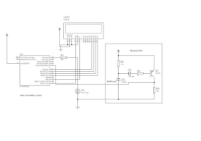
Contact less IR tachometer using PIC16F628A


Tachometer is a device that gives the information about the rotational speed of any shaft or disc. It usually measures the speed in revolutions per minute (RPM). 
I want it to measure the speed of motor so for this i searched the net and found various design but unfortunately they don't worked for me, don't know why?. So i decided to make my own tachometer using PIC16F628A micro-controller and LCD.

Today i am going to make a simple tachometer that could measure the rotation speed of a PC power supply fan without making any physical contact (that's why it is contact less) with the rotating object. The range of this tachometer is 0 - 9999 RPM and displays the RPM on a 16x2 LCD. 

Working operation is simple; IR LED start transmitting and the receiver only receives them when they reflect back. So just count the pulses received and multiply it with 60 to get rpm.  For pulse counter, i am using timer 0 in counter mode.  

Receiver part is build around the receiver LED (photo diode), transistor, and resistor etc. normal condition, the photo diode offers high impedance (as usually used in reversed biased) and so the voltage across it will make the BC557 transistor in the receiver part cut off. The output Pulse will be at logic low. When there is a reflected pulse, the resistance of the photo diode will drop down and allow BC557 transistor to saturate. This gives a logic high Pulse output. The PIC 16F628A will count the pulses within the 1 sec interval to determine the RPM. 

Download: The schematic and code here.
Schematics:
Contact less IR tachometer using PIC16F628A

Snapshot of IR tachometer

Components Required:
U1-------------------------PIC16F628A
R1-------------------------100 ohm
R2-------------------------1.7K ohm
R3-------------------------1K ohm
R4-------------------------10K ohm
D1------------------------- IR LED
D2-------------------------photo diode
D3-------------------------1N4148
Q1--------------------------BC557
Mics:
16x2 LCD
4MHz crystal
22pF ceramic capacitor (2)


Readmore → Contact less IR tachometer using PIC16F628A

Sunday, 5 February 2017

Electronic Project Wind Charger Using LTC1042


Here is a very simple build to electronic circuit project of Wind Charger Circuit Using LTC1042. A very simple wind Charger circuit can be designed using the LTC1042 monolithic CMOS window comparator, manufactured by Linear Technology INC. This Wind charger circuit electronic project use the wind power to produce the energy required to charge Ni-Cd or Lead Acid batteries.

Wind Charger Circuit Diagram:

Charger Circuit Diagram


As you can see in the circuit diagram, you will need an 12 volts generator, a dc motor can be used ( the output voltage is proportional to its rpm).

As you can see in the circuit diagram, are connected two batteries: a 4.5 volts Ni-Cd and a 12 volts Lead Acid battery. If generator voltage output is below 13.8V, the control circuit is active and the NiCad battery is charging through the LM334 current source (the lead acid battery is not being charged).

If the generator voltage output is between 13.8V and 15.1V, the 12V lead acid battery is being charged at about a 1A/hour rate (limited by the power FET). If generator voltage exceeds 15.1V (a condition caused by excessive wind speed or 12V battery being fully charged) then a fixed load is connected thus limiting the generator RPM to prevent damage.


Readmore → Electronic Project Wind Charger Using LTC1042

Saturday, 4 February 2017

Auto Burglar Alarm Using 555 Timer ICs


This electronic circuit project using two 555 timer ICs, Simple circuit and low-cost circuit diagram, basic circuit could be used for a home also.  The circuit Auto burglar alarm will sound your car horn if anyone opens the car door while the circuit is armed. The timers will allow you to leave the car without sounding the horn. To turn the circuit on S1 must be closed.

Auto Burglar Alarm Circuit Diagram:
Alarm

To set the alarm, open S2 (it is normally closed ) this will give you about 5 seconds to get out and close the door. The exit delay time is set by R1 and C1. If anyone opens the doors for more than two seconds the horn will sound until power is removed from the circuit. The 2 second time is set by R2 and C2. If you open the door, you must deactivate the alarm by closing S2.


Readmore → Auto Burglar Alarm Using 555 Timer ICs

Wednesday, 18 January 2017

Automatic Night Light using LDR


Here is the simple Automatic Night Light circuit using LDR.

Components Required:

1) Breadboard
2) 470 ohm resistor
3) 22 Kilo ohm resistor
4) LED (Any Color)
5) 15 Kilo ohm Light Dependent Resistor (LDR)
6) 3904 NPN Transistor
6) 9Volt Battery 

Procedure:
  • Connect the circuit as shown in the circuit diagram below.
  • During day time the brightness will be more, which lowers the resistance of the LDR.
  • Therefore the current is grounded, as current prefers only low resistance path.
  • Hence there is no base current to forward bias the 3904 NPN transistor and the LED remains OFF.
  • During night time the brightness goes down, which increases the resistance of the LDR.
  • Therefore the current will not be grounded and prefers a alternate path to flow.
  • Hence there is enough base current to forward bias the 3904 NPN Transistor and the LED glows.
Circuit Diagram:


Figure 1: Automatic Night Light using LDR Circuit simulation made in Multisim


Figure 2: Automatic Night Light using LDR

Readmore → Automatic Night Light using LDR

Sunday, 15 January 2017

Build a Simple Home Alarm Circuit Using 555 ICs


This is a Simple Home Alarm Circuit Using 555 IC's. This circuit can be simplified by using a single 74C14 IC. This IC is also known by the following numbers: 40106, 40014, and 74HC14.  These are CMOS chips and are characterised by low current consumption, high input impedance and a supply voltage from 5v to 15v. (Do not substitute 7414 or  74LS14. They are TTL chips and operate on 4.5v to 5.5v and have low impedance inputs.)

 Simple Home Alarm Circuit Diagram

Simple Home Alarm Circuit Diagram A


The 74C14 contains 6 Schmitt Trigger gates and 4 of these gates (Schmitt Inverters) are used in this circuit.
The circuit consists of a number of "building blocks" and the first consists of two transistors in a very clever "bootstrap" arrangement. The first transistor is turned on via the 3M3 and 47k. The second transistor is not turned on and the output is HIGH.

A small signal from the electret microphone will consist of positive and negative excursions and the negative excursion will turn the first transistor OFF. This will turn the second transistor ON and the left lead of the 100n will be pulled towards the 0v rail. The 100n is uncharged and the right lead will also be pulled towards the 0v rail and the input of the  74C14 will see a LOW. This will make the output HIGH and turn on the BC547 transistor.

When the second transistor turns ON, it also pulls the 2u2 down and this removes the "turn-on" voltage to the first transistor. The two transistors remain in this state for a few seconds while the 2u2 discharges and the voltage on the base of the first transistor rises. When this happens, the two transistors change state and the 2u2 charges. When the circuit is waiting to detect audio, the 2u2 is charged via the 47k on the base of the first transistor and 47k collector resistor of the second transistor (plus the base-emitter voltage drop of the first transistor).

Simple Home Alarm Circuit Diagram A

Simple Home Alarm Circuit Diagram A

 To exit the property, the EXIT button is pressed and this puts a HIGH on pin 1 of the IC so that any signal from the electret mic is not passed to the siren. The EXIT delay is determined by the value of the 100u and 2M2. Normally-open and normally-closed switches will also send a LOW to trigger the siren.

Readmore → Build a Simple Home Alarm Circuit Using 555 ICs

Saturday, 7 January 2017

Using the high low side driver IR2110 explanation and plenty of example circuits


In many situations, we need to use MOSFETs configured as high-side switches. Many a times we need to use MOSFETs configured as high-side and low-side switches. Such as in bridge circuits. In half-bridge circuits, we have 1 high-side MOSFET and 1 low-side MOSFET. In full-bridge circuits we have 2 high-side MOSFETs and 2 low-side MOSFETs. In such situations, there is a need to use high-side drive circuitry alongside low-side drive circuitry. The most common way of driving MOSFETs in such cases is to use high-low side MOSFET drivers. Undoubtedly, the most popular such driver chip is the IR2110. And in this article/tutorial, I will talk about the IR2110.

You can download the IR2110 datasheet from the IR website. Here's the download link:
www.irf.com/product-info/datasheets/data/ir2110.pdf

First let’s take a look at the block diagram and the pin assignments and pin definitions (also called lead assignments and lead definitions):


Fig. 1 - IR2110 block diagram (click on image to enlarge)


 Fig. 2 - IR2110 Pin/Lead Assignments (click on image to enlarge)


Fig. 3 - IR2110 Pin/Lead Definitions (click on image to enlarge)


Notice that the IR2110 comes in two packages – 14 pin through-hole PDIP package and the 16-pin surface mount SOIC package.

Now let's talk about the different pins.

VCC is the low-side supply and should be between 10V and 20V. VDD is the logic supply to the IR2110. It can be between +3V to +20V (with reference to VSS). The actual voltage you choose to use depends on the voltage level of your input signals. Here’s the chart:


Fig. 4 - IR2110 Logic "1" Input Threshold vs VDD (click on image to enlarge)


It is common practice to use VDD = +5V. When VDD = +5V, the logic 1 input threshold is slightly higher than 3V. Thus when VDD = +5V, the IR2110 can be used to drive loads when input “1” is higher than 3 point something volts. This means that it can be used for almost all circuits, since most circuits tend to have around 5V outputs. When you’re using microcontrollers the output voltage will be higher than 4V (when the microcontroller has VDD = +5V, which is quite common). When you’re using SG3525 or TL494 or other PWM controller, you are probably going to have them powered off greater than 10V, meaning the outputs will be higher than 8V when high. So, the IR2110 can be easily used.

You may lower the VDD down to about 4V if you’re using a microcontroller or any chip that gives output of 3.3V (eg dsPIC33). While designing circuits with the IR2110, I had noticed that sometimes the circuit didn’t work properly when IR2110 VDD was selected as less than +4V. So, I do not recommend using VDD less than +4V.

In most of my circuits, I do not have signal levels which have voltages less than 4V as high and so I use VDD = +5V.

If for some reason, you have signals levels with logic “1” having lower than 3V, you will need a level converter / translator that will boost the voltage to acceptable limits. In such situations, I recommend boosting up to 4V or 5V and using IR2110 VDD = +5V.

Now let’s talk about VSS and COM. VSS is the logic supply ground. COM is “low side return” – basically, low side drive ground connection. It seems that they are independent and you might think you could perhaps isolate the drive outputs and drive signals. However, you’d be wrong. While they are not internally connected, IR2110 is a non-isolated driver, meaning that VSS and COM should both be connected to ground.

HIN and LIN are the logic inputs. A high signal to HIN means that you want to drive the high-side MOSFET, meaning a high output is provided on HO. A low signal to HIN means that you want to turn off the high-side MOSFET, meaning a low output is provided on HO. The output to HO – high or low – is not with respect to ground, but with respect to VS. We will soon see how a bootstrap circuitry (diode + capacitor) – utilizing VCC, VB and VS – is used to provide the floating supply to drive the MOSFET. VS is the high side floating supply return. When high, the level on HO is equal to the level on VB, with respect to VS. When low, the level on HO is equal to VS, with respect to VS, effectively zero.

A high signal to LIN means that you want to drive the low-side MOSFET, meaning a high output is provided on LO. A low signal to LIN means that you want to turn off the low-side MOSFET, meaning a low output is provided on LO. The output on LO is with respect to ground. When high, the level on LO is equal to the level of VCC, with respect to VSS, effectively ground. When low, the level on LO is equal to the level on VSS, with respect to VSS, effectively zero.

SD is used as shutdown control. When this pin is low, IR2110 is enabled – shutdown function is disabled. When this pin is high, the outputs are turned off, disabling the IR2110 drive.
Now let’s take a look at the common IR2110 configuration for driving MOSFETs in both high and low side configurations – a half bridge stage.

 Fig. 5 - Basic IR2110 circuit for driving half-bridge (click on image to enlarge)


D1, C1 and C2 along with the IR2110 form the bootstrap circuitry. When LIN = 1 and Q2 is on, C1 and C2 get charged to the level on VB, which is one diode drop below +VCC. When LIN = 0 and HIN = 1, this charge on the C1 and C2 is used to add the extra voltage – VB in this case – above the source level of Q1 to drive the Q1 in high-side configuration. A large enough capacitance must be chosen for C1 so that it can supply the charge required to keep Q1 on for all the time. C1 must also not be too large that charging is too slow and the voltage level does not rise sufficiently to keep the MOSFET on. The higher the on time, the higher the required capacitance. Thus, the lower the frequency, the higher the required capacitance for C1. The higher the duty cycle, the higher the required capacitance for C1. Yes, there are formulae available for calculating the capacitance. However, there are many parameters involved, some of which we may not know – for example, the capacitor leakage current. So, I just estimate the required capacitance. For low frequencies such as 50Hz, I use between 47µF and 68µF capacitance. For high frequencies like 30kHz to 50kHz, I use between 4.7µF and 22µF. Since we’re using an electrolytic capacitor, a ceramic capacitor should be used in parallel with this capacitor. The ceramic capacitor is not required if the bootstrap capacitor is tantalum.

D2 and D3 discharge the gate capacitances of the MOSFET quickly, bypassing the gate resistors, reducing the turn off time. R1 and R2 are the gate current-limiting resistors.

+MOSV can be up to a maximum of 500V.

+VCC should be from a clean supply. You should use filter capacitors and decoupling capacitors from +VCC to ground for filtering.

Now let’s look at a few example application circuits of the IR2110.

 Fig. 6 - IR2110 circuit for high-voltage half-bridge drive (click on image to enlarge)


 Fig. 7 - IR2110 circuit for high-voltage full-bridge drive with independent switch control (click on image to enlarge)


In Fig. 7 we see the IR2110 being used to drive a full bridge. The functionality is simple and you should understand it by now. A common thing that is often done is that, HIN1 is tied/shorted to LIN2 and HIN2 is tied/shorted to LIN1, enabling the control of all 4 MOSFETs from 2 signal inputs, instead of 4 as shown below in Fig. 8.


 Fig. 8 - IR2110 circuit for high-voltage full-bridge drive with tied switch control - control with 2 input signals (click on image to enlarge)


 Fig. 9 - Using the IR2110 as a single high-voltage high-side driver (click on image to enlarge)


In Fig. 9 we see the IR2110 being used as a single high-side driver. The circuit is simple enough and follows the same functionality described above. One thing to remember is that, since there is no low-side switch, there must a load connected from OUT to ground. Otherwise the bootstrap capacitors can not charge.


 Fig. 10 - Using the IR2110 as a single low-side driver (click on image to enlarge)


 Fig. 11 - Using the IR2110 as a dual low-side driver (click on image to enlarge)


--------------------------------------------------------------------------------------------------------------------------------------------------------------------------------------------------------------

If you've had failures with IR2110 and had driver after driver, MOSFET after MOSFET get damaged, burn and fail, I'm pretty sure that it's due to you not using gate-to-source resistors, assuming of course that you designed the IR2110 driver stage properly. NEVER OMIT THE GATE-TO-SOURCE RESISTORS. If you're curious, you can read about my experience with them here (I have also explained the reason that the resistors prevent damage):

http://www.blogspot.com/2016/10/magic-of-knowledge.html

For further reading, you should go through this:

http://www.irf.com/technical-info/appnotes/an-978.pdf

I have seen in many forums that people struggle with designing circuits with IR2110. I too had a lot of difficulty before I could confidently and consistently build successful driver circuits with IR2110. I have tried to explain the application and use of IR2110 thoroughly through explanation and plenty of examples and hope that it helps you in your endeavors with IR2110.

Readmore → Using the high low side driver IR2110 explanation and plenty of example circuits

Wednesday, 4 January 2017

Inverter as High Voltage Low Current Source Using by 555 timer


This is a simple Electronic Circuit Projects of  Inverter as high voltage low current source using by 555 timer IC. The circuit is capable of providing power for portable Geiger counters, dosimeter chargers, high resistance meters, etc.

Inverter as High Voltage Low Current Source Circuit Diagram:

Inverter Circuit Diagram

The 555 timer IC is used in its multivibrator mode, the frequency adjusted to optimize the transformer characteristics. When the output of the IC is high, current flows through the limiting resistor, the primary coil to charge C3. When the output is low, the current is reversed With a suitable choice of frequency and C3, a good symmetric output is sustained.

Readmore → Inverter as High Voltage Low Current Source Using by 555 timer

Tuesday, 20 December 2016

Light Level Indicator Using a Window Comparator


The second example below uses a LDR (light dependent resistor) to indicatesome desired light level. The LDR has a large dynimic range and varies inresistance from less than 100 ohms on a cloudy day to over a megohm in totaldarkness. A 2K pot was used to adjust the window range for usual room lightconditions. This setup might also be used to indicate sunrise/sunset conditions.

Light Level Indicator Circuit Diagram

Light Level Indicator Circuit Diagram

The proto board picture below shows the circuit wired to measure lightlevel using a LDR and 2K potentiometer. The green (window) LED is litindicating the light level is about right to take the picture.


Indicator Circuit Diagram


Readmore → Light Level Indicator Using a Window Comparator

Sunday, 18 December 2016

Sooper Amplifier Using BEL1895 I C


Here is a very simple and easy to use audio amplifier using I.C BEL(Bharat electronics limited)1895 , a very common IC. This circuit can run on 3V to 6v , making it easy to use in pocket amplifier. Cost is under 25/-
Sooper Amplifier Using BEL1895 I.C


Parts list:

BEL1895 I.C (DIP8),
C1 = 470uF/10V,
C2 = 1000uF/16V,
C3 = 220uF/10V,
C4 = 100uF/10V,
C5 = 4.7uF/10V,
C6 = 47pF,
C7,C8 = 1uF,
R1 = 47Ohm,
R2 = 470Ohm,
R3 = 100K,
R4 = 1Ohm,
R5 = 10K V/C,
speaker, etc…
Total cost is around 20-30 rupeess(INR) or 0.6USD. 

Readmore → Sooper Amplifier Using BEL1895 I C

Friday, 16 December 2016

Stepper Motor Controller Using by A3952S


Using the A3952S stepper motor controller ( designed by Allegro MicroSystems ) we can design a very simple and useful motor driver circuit that can be used in many electronic applications . A3952S stepper motor controller is capable of continuous output currents up to 2 A and operating voltages range up to 50 V. Internal fixed off-time PWM current-control circuitry can be used to regulate the maximum load current to a desired value. The MODE terminal can be used to optimize the performance of the device in microstepping / sinusoidal stepper motor drive applications.

A3952S Stepper Motor Controller Circuit diagram


When the average load current is increasing, slow-decay mode is used to limit the switching losses in the device and iron losses in the motor. The thermal performance in applications with high load currents and/or high duty cycles can be improved by adding external diodes in parallel with the internal diodes. In internal PWM slow-decay applications, only the two top-side (flyback) diodes need be added. For internal fast-decay PWM, or external PHASE or ENABLE input PWM applications, all four external diodes should be added for maximum junction temperature reduction .

As you can see in the schematic diagram , this stepper motor driver circuit require two A3952S circuits and other few additional electronic components.

Readmore → Stepper Motor Controller Using by A3952S

Thursday, 8 December 2016

Voltage Inverter using IC NE555


In many circuits we need to generate an internal adjustable voltage. This circuit shows how it is possible to use a trusty old NE555 timer IC and a bit of external circuitry to create a voltage inverter and doubler. The input voltage to be doubled is fed in at connector K1. To generate the stepped-up output at connector K2 the timer IC drives a two-stage inverting charge pump circuit.

The NE555 is configured as an astable multivibrator and produces a rectangular wave at its output, with variable mark-space ratio and variable frequency. This results in timing capacitor C3 (see circuit diagram) being alternately charged and discharged; the voltage at pin 2 (THR) of the NE555 swings between one-third of the supply voltage and two-thirds of the supply voltage.

Voltage Inverter Circuit Using IC NE555

The output of the NE555 is connected to two voltage inverters. The first inverter comprises C1, C2, D1 and D2. These components convert the rectangular wave signal into a nega-tive DC level at the upper pin of K2. The second inverter, comprising C4, C5, D3 and D4, is also driven from the output of IC1, but uses the negative output voltage present on diode D3 as its reference potential. The consequence is that at the lower pin of output connector K2 we obtain a negative volt-age double that on the upper pin.


Now let us look at the voltage feedback arrangement, which lets us adjust this doubled negative output voltage down to the level we want. The NE555 has a control voltage input on pin 5 (CV). Normally the voltage level on this pin is maintained at two-thirds of the supply voltage by internal circuitry. The voltage provides a reference for one of the comparators inside the device. If the reference voltage on the CV pin is raised towards the supply voltage by an external circuit, the timing capacitor C3 in the astable multivibrator will take longer to charge and to discharge. As a result the frequency of the rectangle wave output from IC1 will fall, and its mark-space ratio will also fall.

The source for the CV reference voltage in this circuit is the base-emitter junction of PNP transistor T1. If the base volt-age of T1 is approximately 500 mV lower than its emitter voltage, T1 will start to conduct and thus pull the voltage on the CV pin towards the positive supply.

In the feedback path NPN transistor T2 has the function of a voltage level shifter, being wired in common-base configuration. The threshold is set by the resistance of the feedback chain comprising resistor R3 and potentiometer P1. When the emitter voltage of transistor T2 is more than approximately 500 mV lower than its base voltage it will start to conduct. Its collector then acts as a current sink. Potentiometer P1 can be used to adjust the sensitivity of the negative feedback circuit and hence the final output voltage level.Using T1 as a voltage reference means that the circuit will adjust itself to compensate not only for changes in load at K2, but also for changes in the input supply voltage. If K2 is disconnected from the load the desired output voltage will be maintained, with the oscillation frequency falling to around 150 Hz.

A particular feature of this circuit is the somewhat unconventional way that the NE555’s discharge pin (pin 7) is connected to its output (pin 3). To understand how this trick works we need to inspect the innards of the IC. Both pins are outputs, driven by internal transistors with bases both connected (via separate base resistors) to the emitter of a further transistor. The collectors of the output transistors are thus isolated from one another [1].

The external wiring connecting pins 3 and 7 together means that the two transistors are operating in parallel: this roughly doubles the current that can be switched to ground.The two oscilloscope traces show how the output voltage behaves under different circumstances. The left-hand figure shows the behaviour of the circuit with an input voltage of 9 V and a resistive load of 470 Ω connected to the lower pin of output connector K2. The figure on the right shows the situation with an input voltage of 10 V and a load of 1 kΩ on the lower pin of output connector K2. The pulse width and frequency of the rectangle wave at the output of IC1 are automatically adjusted to compensate for the differing conditions by the feedback mechanism built around T1 and T2.

Because of the voltage drops across the Darlington out-put stage in the IC (2.5 V maximum) and the four diodes (700 mV each) the circuit achieves an efficiency at full load (470 Ω between the output and ground) of approximately 50 %; at lower loads (1 kΩ) the efficiency is about 65 %.

Author : Peter Krueger -  Copyright : Elektor

Readmore → Voltage Inverter using IC NE555

Saturday, 3 December 2016

Simple Six way Switch Using IC1 40106N


The 40106 is a versatile CMOS IC containing six Schmitt trigger inverters. It can be used to implement a set of alternating –action switches with hard ware contact bounce suppression.

Simple Six-way Switch Circuit Diagram :

Simple Six-way-Switch-Circuit Diagram

Aside from one gate of the IC, all you need for each switch is a pushbutton, a resistor and two capacitors. It works as follows. The 1 μF capacitor at the output is charged or dis-charged via a 1 MΩ resistor, depending on the output level of the inverter.

Pressing the button causes the input level of the gate to change, which in turn causes the output level to toggle. The 10 nF capacitor determines the output state after the supply voltage is switched on. You can connect it to the supply voltage rail or the ground rail as required. If you hold the button pressed, the output signal will be a square wave with a frequency determined by the RC time constant, which is approximately 1 second.

You may experiment with the component values if you wish.


Author : Kees van het Hoff - Copyright : Elektor


Readmore → Simple Six way Switch Using IC1 40106N

Sunday, 20 November 2016

TRANSISTOR TESTER CIRCUIT USING NE555


Readmore → TRANSISTOR TESTER CIRCUIT USING NE555

Thursday, 17 November 2016

Electronic Power Flip Flop Using A Triac Circuit Diagram


This is a project of Electronic Power Flip-Flop Using A Triac Circuit Diagram. Modern electronics is indispensable for every large model railroad system, and it provides a solution to almost every problem. Although ready-made products are exorbitantly expensive, clever electronics hobbyists try to use a minimum number of components to achieve optimum results together with low costs. This approach can be demonstrated using the rather unusual semiconductor power flip-flop described here. A flip-flop is a toggling circuit with two stable switching states (bistable multivibrator). It maintains its output state even in the absence of an input pulse.

Flip-flops can easily be implemented using triacs if no DC voltage is available. Triacs are also so inexpensive that they are often used by model railway builders as semiconductor power switches. The decisive advantage of triacs is that they are bi-directional, which means they can be triggered during both the positive and the negative half-cycle by applying an AC voltage to the gate electrode (G). The polarity of the trigger voltage is thus irrelevant. Triggering with a DC current is also possible. Figure 1 shows the circuit diagram of such a power flop-flop. A permanent magnet is fitted to the model train, and when it travels from left to right, the magnet switches the flip-flop on and off via reed switches S1 and S2.

Power Flip-Flop Using A Triac Circuit diagram:

Electronic Power Flip-Flop Using A Triac Circuit Diagram

In order for this to work in both directions of travel, another pair of reed switches (S3 and S4) is connected in parallel with S1 and S2. Briefly closing S1 or S3 triggers the triac. The RC network C1/R2, which acts as a phase shifter, maintains the trigger current. The current through R2, C1 and the gate electrode (G) reaches its maximum value when the voltage across the load passes through zero. This causes the triac to be triggered anew for each half-cycle, even though no pulse is present at the gate. It remains triggered until S2 or S4 is closed, which causes it to return to the blocking state.The load can be incandescent lamps in the station area (platform lighting) or a solenoid-operated device, such as a crossing gate. The LED connected across the output (with a rectifier diode) indicates the state of the flip-flop. 

The circuit shown here is designed for use in a model railway system, but there is no reason why it could not be used for other applications. The reed switches can also be replaced by normal pushbutton switches. For the commonly used TIC206D triac, which has a maximum current rating of 4 A, no heat sink is necessary in this application unless a load current exceeding 1 A must be supplied continuously or for an extended period of time. If the switch-on or switch-off pulse proves to be inadequate, the value of electrolytic capacitor C1 must be increased slightly.
Author: R. Edlinger - Copyright: Elektor July-August 2004

Readmore → Electronic Power Flip Flop Using A Triac Circuit Diagram