Showing posts with label power. Show all posts

Friday, 24 March 2017

17 Watt dual BTL Audio Power Amplifier HA13127


17 Watt dual BTL Audio Power Amplifier HA13127
Datasheet for HA13127: Download
Readmore → 17 Watt dual BTL Audio Power Amplifier HA13127

Thursday, 23 March 2017

12 Volt 2 A Switching Power Supply Circuit Diagram


This is a Simple 12 Volt / 2 A Switching Power Supply Circuit Diagram. The circuit 12 volt / 2 A switching power supply in the above scheme is not too complicated. At the output of this block provides a stable 12 V and maximum current 2A. Power supply units are quite compact and is suitable for debugging schemes, as well as a permanent resource for stationary devices, including power for the logic electronics for the home-made ​​CNC machine tools. 

Circuit Diagram


12 Volt / 2 A Switching Power Supply Circuit Diagram


Transformer is available in the free market and avoids the hassle of having to self-winding. The diode bridge BR 1 of any given voltage and current of 2A. All other elements in the high part of the circuit are designed by the same voltage, taking into account the mains. The scheme of 12 volt / 2 A switching power supply operates from the high voltage network, to be observed when mounting accuracy and caution when using. It is desirable to block the finished board to “pack” in the body. 
Readmore → 12 Volt 2 A Switching Power Supply Circuit Diagram

AC Power Control with Thyristor Phase Angle Control using triac with PIC16F877A


Principle of Phase Angle Control
Top - Output Voltage
Bottom - Gate Drive Signal
Image source: Wikipedia (http://en.wikipedia.org/wiki/File:Regulated_rectifier.gif)


The photo above clearly illustrates phase angle control: output voltage controlled by the gate drive signal applied to a thyristor. What is phase angle control? That is what I'm going to talk about in this article.

Phase angle control is a method of PWM applied to AC input voltages, usually the mains supply. Of course, the AC supply could be from a transformer or any other AC source, but the mains supply is the most common input – this gives the phase angle control method its greatest usefulness. It has of course become quite obvious from the title (and I’m sure most of you reading will already know this) that the purpose of phase angle control is to control or limit power to the load.

The power device used in phase angle controllers is a thyristor – mostly triacs or SCRs. (There are methods of phase controlling employing high frequency switching using a MOSFET or IGBT, but here I’ll talk about phase angle control with thyristors only). The power flow to the load is controlled by delaying the firing angle (firing time each half-cycle) to the power device.

We know that the thyristor is a latching device – when the thyristor is turned on by a gating signal and the current is higher than the holding current and the latching current, the thyristor stays on, until the current through it becomes sufficiently low (very close to zero). The thyristor turns off when current through it becomes zero, as happens at the AC mains zero crossing. This is the natural line commutation. (Another method of turning the thyristor off is by forced commutation. I won’t go into that now.) The assumption here is that the load is resistive and has little to no inductance. Of course, this is not always the case, as inductive loads are often used. However, I’ll work with this assumption for now.

Now, with that covered, you should read this article first before proceeding to the rest of this article:

Zero crossing detection with PIC16F877A:  http://www.blogspot.com/2016/10/zero-crossing-detection-with-pic16f877a.html

I’ve added the circuit, code and simulation of an example later in this article. And that uses a triac as the power device. So, from now on, I’ll just refer to the triac instead of talking about a thyristor in general.

So, in phase angle control, a gate pulse is sent to the triac. This is sent at a time between one zero crossing and the next. Without the gate pulse sent to the triac, right after zero-crossing, the triac is off and no current flows through it. After a certain time, the gating signal is given to the triac and it turns on. The triac then stays on until the current through it becomes zero (natural line commutation). This is at the next zero crossing. For simplicity’s sake and as usually should be, assume that the current through the triac (when on) is larger than the latching current and the holding current. If you didn’t already know this, the latching current is the current that must pass through the triac right after it is turned on to ensure that it latches. The holding current is the current level through the triac below which the triac will turn off. So, the assumption that current through the triac is higher than the latching current and the holding current means that the triac stays on once it is fired on. It stays on until the current through it is zero.

This means that the voltage is supplied to the load for a fraction of the cycle, determined by how long the triac is on. How long the triac is on, is, in turn, determined by the delay time between the zero-crossing and the applying of the triac gating signal.

So, to sum it up, we adjust the voltage or power delivered to the load by delaying the trigger signal to the triac. One thing to remember is that, the delivered voltage and power are not linearly related to the firing phase angle.

There are two voltages here that we are concerned with – the RMS voltage and the average voltage. The RMS voltage governs the power output to resistive loads such as incandescent bulbs and resistive heaters. The average value relates to devices that function on the average voltage level. This is important because, when testing, your voltmeter will register the average voltage – and not the true RMS voltage – unless you have a “true RMS voltmeter”. Most inexpensive voltmeters are not true RMS meters but will respond to average value changes.

To clarify why power and voltage are not linearly related, let’s examine the formula relating the two.
 
So, assuming a constant resistance (be careful if you’re using incandescent lamps, since they are NOT constant resistance devices), power is directly proportional to the square of the voltage. So, if you half the voltage, the power is not halved, but is reduced to one-fourth the original power! One-fourth power with half the voltage!

Now let’s now go on to the design part – how we’re actually going to do this.
For the microcontroller, I’ve chosen the extremely popular PIC 16F877A. However, since this application requires only a few pins, you can easily use any other small microcontroller for this purpose, such as PIC 12F675.

The zero-crossing is done using the bridge-optocoupler method as I had previously shown. For details regarding the zero-crossing, please go through the article:
Zero crossing detection with PIC16F877A:  http://www.blogspot.com/2016/10/zero-crossing-detection-with-pic16f877a.html

Now, let’s take a look at the code:
//---------------------------------------------------------------------------------------------------------
//Programmer: Syed Tahmid Mahbub
//Compiler: mikroC PRO for PIC v4.60
//Target PIC: PIC16F877A
//Program for phase angle control
//---------------------------------------------------------------------------------------------------------
unsigned char FlagReg;
sbit ZC at FlagReg.B0;

void interrupt(){
     if (INTCON.INTF){          //INTF flag raised, so external interrupt occured
        ZC = 1;
        INTCON.INTF = 0;
     }
}

void main() {
     PORTB = 0;
     TRISB = 0x01;              //RB0 input for interrupt
     PORTA = 0;
     ADCON1 = 7;                 //Disable ADC
     TRISA = 0xFF;                                //Make all PORTA inputs
     PORTD = 0;
     TRISD = 0;                 //PORTD all output
     OPTION_REG.INTEDG = 0;      //interrupt on falling edge
     INTCON.INTF = 0;           //clear interrupt flag
     INTCON.INTE = 1;           //enable external interrupt
     INTCON.GIE = 1;            //enable global interrupt

     while (1){
           if (ZC){ //zero crossing occurred
              delay_ms(2);
              PORTD.B0 = 1; //Send a pulse
              delay_us(250);
              PORTD.B0 = 0;
              ZC = 0;
           }
     }
}

There isn’t much to it. The zero-crossing is first checked. After zero-crossing occurs, a small delay is present before the triac is fired. Here, I’ve used 2ms. So, the triac is fired 2ms after the zero-crossing occurs. The gating signal is removed 250µs after that. 250µs is enough time to ensure that the triac has turned on. Even though the gating signal is removed, the triac stays on until the next zero-crossing as it is a latching device. Now you may ask, why remove the gating signal? Just keep it on till the next zero-crossing. Well, that'd work too. The problem there would be that, there would be high switching losses of the thyristor. The gate drive resistance would dissipate immense amounts of power - all for no reason, since the triac would be on even if the signal was removed.

The rest of the code should be easy to understand and should be self-explanatory – I’ve added comments to help you understand.

Now let’s take a look at my circuit setup and then the output waveform using this code:

Fig. 1 - Circuit Diagram (Click on image to enlarge)


You should choose R1 depending on the gate current requirements of the triac. It must also have a sufficiently high power dissipation rating. Usually, the instantaneous power may be very high. But since current flows through the resistor for only 250us (1/40 of a 50Hz half cycle), the average power is small enough. Usually, 2W resistors should suffice.

Let’s assume we’re using a BT139-600 triac. The maximum required trigger current is 35mA. Although the typical trigger current is lower, we should consider the maximum required trigger current. This is 35mA for quadrants I, II and III. We will only be firing in quadrants I and III. So, that is ok for us – we need to consider 35mA current.

If you aren’t sure what quadrants are, here’s a short description. First take a look at this diagram:

 Fig. 2 - Triac Triggering Quadrants


If you look back again at the diagram, you’ll see that we’re driving gate from MT2. So, we can say that, with respect to MT1, when MT2 is positive, so is the gate. With respect to MT1, when MT2 is negative, so is the gate. From the diagram above, you can see that these two cases are in quadrants I and III. This is what I meant when I mentioned that we’re driving only in quadrants I and III.


The driver in the circuit is the MOC3021. This is a random phase optically isolated triac output driver. When the LED is turned on, the triac in the MOC3021 turns on and drives the main triac in the circuit. It is a “random phase” driver meaning that it can be driven on at any time during the drive signal, as is required for phase angle control. There are other drivers that only allow drive at the zero-crossing. These cannot be used for phase angle control as phase angle control requires drive after zero-crossing. For guaranteeing that the triac is latched, the LED side of the MOC3021 must be driven with at least 15mA current. The maximum current rating for the LED is 60mA. The peak current rating for the triac is 1A. You should find that we have stayed within these limits in the design.

Here’s the output waveform:
 Fig. 3 - Triac firing with 2 ms delay

Green: Input AC
Yellow: AC Output after phase angle control
Pink: Gate Drive signal


You can clearly see that before the gate driving signal is applied, there is no output (illustrated by the flat yellow line).When the gate driving signal is applied, the triac turns on. There is an output and the triac stays on till the next zero crossing. After this again, there is no output till the next gate drive signal is applied.

Now I’ll show you a few more waveforms, with other initial delays.

Here, the gate is driven 1ms after the zero-crossing:
 Fig. 4 - Triac firing with 1 ms delay

Green: Input AC
Yellow: AC Output after phase angle control
Pink: Gate Drive signal


Here, the gate is driven 4ms after the zero-crossing: 
 Fig. 5 - Triac firing with 4 ms delay

Green: Input AC
Yellow: AC Output after phase angle control
Pink: Gate Drive signal


Here, the gate is driven 5ms after the zero-crossing:
 Fig. 6 - Triac firing with 5 ms delay

Green: Input AC
Yellow: AC Output after phase angle control
Pink: Gate Drive signal


Here, the gate is driven 6ms after the zero-crossing:
Fig. 7 - Triac firing with 6 ms delay

Green: Input AC
Yellow: AC Output after phase angle control
Pink: Gate Drive signal

Now, to finish things off, I’ll show you how to find the RMS value of the output voltage.

We first need to know how to relate the firing delay with firing angle. We know that one complete sine wave is 360°. That is 2πradians. We then need to know that the firing angle α = ωt, where ω = 2πf. Since, we’re working with 50Hz here, f=50Hz. Thus, ω = 100π. Just to test this relationship, let’s use t = 0.020 seconds (20ms). Thus α = 100π * 0.020 = 2π, as told before.

So, if we’re firing at a delay of 4ms, that is 4ms after the zero crossing, the firing angle α = 100 π * (4/1000) = 0.4 π (in radians obviously).

The RMS output voltage is found from the relationship:


So, if we are firing after 4ms, (α = 0.4 π), the output RMS voltage is:


Remember, at the beginning, I mentioned that the voltage output is not linearly correlated with the firing angle? This is what I meant. Here, the delay is 4ms. So, the triac is on for 60% of the cycle. But the output RMS voltage is 183.2V - 83% of the input voltage. The lack of direct proportionality is evident here. The reason behind this is the shape of the AC - sinusoidal.

Now, I give you the task of finding the RMS voltage for the other cases mentioned in this tutorial.

If you want to then find power, you can use the relationship P = V2/R to find the power. The assumption here is that the resistance is constant, as was assumed at the beginning of the tutorial. If the resistance is not constant, power will still vary will resistance, just not directly proportionally.


Here in this article, I’ve talked about phase angle control with some background information on triacs. I’ve shown how to implement phase angle control with a PIC and also how to calculate the RMS voltage of the output. I hope I’ve been able to explain this extremely important topic to you clearly and hope that you can now successfully build your own power control circuits using phase angle control with triacs.

Reference Book:
One of the best books for understanding the theory behind phase angle control is "POWER ELECTRONICS - CIRCUITS, DEVICES AND APPLICATIONS" by Muhammad H. Rashid. If you want to learn more about thyristors or phase angle control, I recommend reading this book for more info.
Readmore → AC Power Control with Thyristor Phase Angle Control using triac with PIC16F877A

Wednesday, 22 March 2017

Adjustable switching power supply


Adjustable switching power supply

This circuit supplying current maximum10A with an adjustable output voltage from 0-25 VDC. Adjustable Switching Regulator L4970 Series is built with the main component as a Switching Regulator IC L4970.


Switching Regulator L4970 series include not complicated to make his own, which need to be considered is the IC L4970 require sufficient cooling to operate in an optimal and durable. Adjustable Switching Regulator L4970 series are complete can be seen in thethe following figure .

Adjustable switching power supply
Adjustable switching power supply schematics

To set the output voltage range Adjustable Switching Regulator L4970 can be in control by adjusting the potentiometer 18KOhm tus.

Readmore → Adjustable switching power supply

Friday, 17 March 2017

30W Power Audio Amplifier Circuit Diagram


TIP141 si a npn silicon power darling tons designed for complementary use with TIP145, TIP146 and TP147. Can stand up to 125 W at 25°C Case Temperature, 10 A Continuous Collector Current and has a minimum hFE of 1000 at 4 V, 5 A. This home audio amplifier can output 30W with a +- 32V symmetric power supply. If you want a stereo power amplifier please check out the other schematics.


R1=1Kohm R16-17=270ohm D1=9.1V 0.4W zener
R2=47Kohm R18=22ohm 1W D2-3=1N4148
R3=1.5Kohm R19=NC Q1-2=BC550C
R4-5=10Kohm R20-21=0.39ohm 4W Q3=MPSA56
R6=5.6Kohm TR1=250ohm trimmer Q4=BC547B
R7=10ohm C1=470nF 100V MKT Q5=BC212
R8=47Kohm C2=1nF 100V MKT Q6=BC183
R9=560ohm C3=68pF ceramic Q7-8=MPSAO6
R10-11=8.2Kohm C4-8=22nF 100V MKT Q9=TIP141
R12-15=120ohm C5-6-7=100nF 100V MKT Q10=TIP146
R13=680ohm C9=47uF 25V F1-2=1.6AT FUSE
R14=330ohm C10-11=220uF 63V All the resistors is 1/4W 1% except quote differently

30W power amplifier circuit diagram

30W power amplifier circuit diagram

30 Watt audio amplifier PCB

30 Watt audio amplifier PCB


Readmore → 30W Power Audio Amplifier Circuit Diagram

TA8210AH Stereo Car Power Amplifier


IC TA8210AH By using this you can apply a series of audio power amplifier is the car audio system. In general, all the speakers in the car using a subwoofer speaker, and woofer. Because the car is not big room so the sound is being required is not too high.

Audio amplifier circuit can work at a minimum voltage 12-volt DC, if supplied under voltage 12-volt amplifier work will be less than the maximum. This amplifier output power up to 200W or 2 x 100W stereo with 8 ohm impedance.


200W car amplifier schematic

Part List :

Resistor

R1 =1K

R2 =50K trim

R3 =1K

R4 =50K trim

R5 =680R

R6 =680R

R7 =150K

R8 =2R2

R9 =2R2

R10=2R2

R11=2R2


Capacitor

C1 =1uF

C2 =1uF

C3 =47uF

C4 =47uF

C5 =100n/400V

C6 =220uF

C7 =220uF

C8 =100n/400V

C9 =100n/400V

C10=100n/400V


Intregated Circuit

IC1=TA8210AH


Connector

X2-3=in R

X2-2=gnd

X2-1=in L

X1-1,X1-2=Out R

X1-3,X1-4=Out L
Readmore → TA8210AH Stereo Car Power Amplifier

Wednesday, 15 March 2017

Adjustable Voltage Current Power Supply Circuit Using IC L200


IC2 is connected as a differential amplifier and compares the signals at its two inputs.
Referring to the circuit diagram: the input comprises a mains switch, fuse, transformer, bridge rectifier and smoothing capacitor (C2). 


The difference between the inputs is the voltage drop across 'current’ sensor R4. This IC feeds the current sensing input (pin 2) of the L200. 


P1 in the feedback loop of the 741 is used to vary the output current of the circuit. IC1 must be mounted on a suitable heat sink as it dissipates nearly all the power of the circuit.
The reference level output from I pin 4 of IC1 goes to the voltage divider made up of R5 and P2 (this pot sets the value of the output voltage).


The power supply can quite easily be built into a case and a voltmeter and ammeter mounted on the front panel. ln view of the accuracy of the circuit these should ideally be digital meters, but virtually any type will do.


If you compare the expense and the rating of this power supply you will get a surprise, because the output voltage and current are fully adjustable between O. . . 18 V and 0 . . . 1.8 A respectively and costs have still been kept very reasonable. 


Diode D5 and capacitor C1 produce a negative auxiliary voltage, which is stabilized by zener diode D6 and capacitor C4. 


All this is necessary to enable the output voltage to be adjusted down to zero volts. During the construction of this part of the circuit bear in mind that the positive lead of electrolytic capacitor C4 is connected to earth! Regulation is provided by IC1 and IC2. Capacitor C3 suppresses any residual transients at the input of lC1 and it should therefore be connected as closely as possible to IC1 similarly C4 and IC2). 


The negative voltage provides the negative supply for the two ICs.


 Adjustable Voltage, Current Power Supply Circuit Using IC L200

Readmore → Adjustable Voltage Current Power Supply Circuit Using IC L200

Friday, 10 March 2017

Low ripple power supply schematic


Simple schematic above is a circuit of power supply that can operate at high current with very small ripple voltage. How it works similiar to the high power class AB amplifiers, with the same quality. T1,T2 ,and R2 can also be called a power NPN-Darlington transistor. ZD1 and R1 as a supplier of voltage on the transistor base and filtered by C2. ZD1 can be slected with formulated (Figure 1.0) . For the C2 can be selected in accordance with the degree of smoothness as its value is effectively combined with the multiplied gain of the Transistor T1 and T2, assumsing minimum hfe for T1 and T2 , C=100x15(T1) x 25 (T2) = 37,000uF, adjust the voltage C2 with the input voltage, but must be higher than input voltage.
Low ripple power suplly regulator
Part List :
R1 = 2K2
R2 = 56R
R3 = 10K
C1 = 1500uF
D1-D4 = Didode 6A
T1 = 2N3054
T2 = 2N3055
rumus tegangan ripple
Figure 1.0

Readmore → Low ripple power supply schematic

power circuit diagram of star delta starter


Readmore → power circuit diagram of star delta starter

Saturday, 4 March 2017

LM338 Power Supply 13 8V 5A


This ac to dc power supply can output 5A in continous operation and 12A peak current. This kind of dc power supplies uses a PCB so you can use two case types for IC1, TO-220 or TO-3. The regulation of this 12 volt power supply is made with TR1 ( multiturn ). IC1 must be placed on proper heatsink.

LM338 Power Supply Circuit Diagram :


 13.8V 5A power sp-Circuit Diagram

Readmore → LM338 Power Supply 13 8V 5A

Friday, 24 February 2017

Simple Audio Power Meter Circuit


This simple circuit indicates the amount of power that goes to a loudspeaker. The dual-color LED shows green at an applied power level of about 1 watt. At 1.5 watts it glows orange and above 3 watts it is bright red. The circuit is connected in parallel with the loudspeaker connections and is powered from the audio signal. The additional load that this represents is 470 Ohm (R1//R3) will not be a problem for any amplifier. During the positive half cycle of the output signal the green LED in the dual-color LED will be turned on, provided the voltage is sufficiently high.

At higher output voltages, T1 (depending on the voltage divider R2/R1) will begin to conduct and the green LED will go out. During the negative half cycle the red LED is driven via R3 and will turn on when the voltage is high enough. In the transition region (where T1 conducts more and more and ‘throttles’ the green LED as a result) the combination of red/green gives the orange colour of the dual-LED. By choosing appropriate values for the resistors the power levels can be adjusted to suit.
Audio Power Meter Circuit Diagram


The values selected here are for typical living room use. You will be surprised at how loud you have to turn your amplifier up before you get the LEDs to go! The resistors can be 0.25 W types, provided the amplifier does not deliver more than 40 W continuously. Above this power the transistor will not be that happy either, so watch out for that too. Because T1 is used in saturation, the gain (Hfe) is not at all important and any similar type can be used. The power levels mentioned are valid for 4-Ohm speakers. For 8-Ohm speakers all the resistor values have to be divided by two.


Readmore → Simple Audio Power Meter Circuit

Friday, 17 February 2017

Power up down Sequencer


Power-up/down Sequencer Circuit Diagram. Whether you’re talking about a home cinema  or a computer system, it’s very often the case  that the various elements of the system have  to be turned on or off in a quite specific order,  or at least, automatically. Constructing this  sort of automation system is well within the  capability of any electronics enthusiast worthy of the name, but in this ‘all-digital’ age,  most of the circuits of this type to be found  in amateur electronics magazines or web-sites use a microcontroller. Even though that  is indeed a logical solution (in  more ways than one!), and you  might even say the easiest one, it  does pose problems for all those  people who don’t (yet) have the  facilities for programming these  types  of  IC.  So  we  decided  to  offer you now an approach that’s  very different, as it only uses a  simple, cheap, commonly-avail-able analogue integrated circuit,  which of course doesn’t have to  be programmed. Our project in  fact uses as it’s ‘brain’ an LM3914,  a familiar IC from National Semiconductors,  usually  used  for  driving  LED  VU  (volume  unit)  meters. 


Power-up-down Sequencer Circuitw
Power-up/down Sequencer Circuit Diagram

Before taking a look at the circuit  for  our  project,  let ’s  just  remind ourselves that the IC has  one analogue input and ten out-puts intended for driving LEDs.  It can operate in ‘point’ mode,  where the LEDs light up in turn,  from first to last, depending on  the input voltage, but only one LED is lit at  any given time. Alternatively  it can operate  in ‘bar’ mode (this is the mode normally used  for VU meters), and in this case, the LEDs light  up one after the other, in such a way as to create a strip of light (bar) that is longer or  shorter according to the input voltage. This is  the mode selected for the LM3914 in the circuit described in some detail below. 

So as to be able to control the AC powered equipment  our  sequencer  is  intended  to manage, we are using solid-state relays — four, in our example, though you can reduce or increase this number, up to a maximum of ten. Since the input devices in solid-state relays are LEDs, they can be driven directly by the LM3914 outputs, since that’s exactly what they’re designed for. As only four relays  are available, these are spread across out-puts L2, L4, L6, and L8, but you can choose  any arrangement you like to suit the number  of relays you want to use. 

Resistor R7 connected to pin 7 of the LM3914  sets the current fed to the LEDs by the LM3914  outputs. Here, it’s been set to 20 mA, since  that is the value expected by the solid-state  relays chosen. The input voltage applied to  pin 5 of the LM3914 is none other than the  voltage present across capacitor C1 — and  this is where the circuit is ingenious. When  the switch is set to ‘on’, C1 charges slowly  through R5, and the LEDs of the solid-state  relays on the outputs light one after another  as this voltage increases; in this way, the units  being controlled are powered up in the order you’ve chosen. To power-down, all you have  to do is flip the switch so that C1 discharges  through  R5,  and  the  LEDs  go  out  in  the  reverse order to that in which they were lit,  in turn powering down the units connected to the solid-state relays. Easy, isn’t it? If you’re not happy with the sequence speed,  all you need do is increase or reduce the  value of R5 in order to alter the speed one  way or the other.
The circuit needs to be powered from a volt-age of around 9 to 12 V, which doesn’t even  need to be stabilized. A simple ‘plug-top’,  ‘wall wart’ or ‘battery eliminator’ unit will be  perfect, just as long as it is capable of supply-ing enough current to power all the LEDs. As  the LED current is set by R7 to 20 mA per LED,  it’ll be easy for you to work out the current  required, according to the number of solid-state relays you’re using. 

In our prototype the type S216S02 relays  from Sharp were used, mainly because they  proved readily available by mail order. They also have the advantage of being compact,  and their switching capacity of 16 A means  you can dispense with a heatsink if you’re  using them for a computer or home cinema  system, where the current drawn by the vari-ous units can be expected to remain under  1 A. These solid-state relays must be protected by a fuse, the rating of which needs to  be selected according to the current drawn  by the devices being powered. 

Also note the presence across the relay terminals of a VDR, also known as a GeMOV or  SiOV, intended to protect them from any spurious voltage spikes. You can use any type  that ’s intended for operation on 250 VAC  without any problem. The values of fuses F1  to F4 are of course going to depend on the  load being protected. 

Construction of the circuit shouldn’t present any particular difficulty, but as the solid-state relays are connected directly to AC  power, it is essential to install it in a fully-insulated case; the case can also be used to  mount the power outlet sockets controlled  by the circuit. Note that sockets are female  components.
Let’s just end this description with the sole  restriction imposed by our circuit — but it’s  very easy to comply with, given the intended  use. In order to remain triggered, the solid-state relays must carry a minimum holding  current, which is 50 mA in the case of the  devices we’ve selected. In practical terms,  this just means that each of the devices powered by our sequencer must draw at least  50 mA, or in other words roughly 12 VA at  230 VAC, or 25 VA at 120 VAC.

Author :Christian Tavernier

Readmore → Power up down Sequencer

Thursday, 9 February 2017

Electronic Circuit Project of Power Loss Detector


Here is a simple Electronic Circuit Project of Power loss detector Circuit Diagram. A positive going input charges C through the IN4148 and R.

Power Loss Detector Circuit Diagram:

Electronic Circuit Project

The diode keeps the scs off. A negative going input supplies anode-gate current triggering on the scs discharging C through Rl.

Readmore → Electronic Circuit Project of Power Loss Detector

Wednesday, 1 February 2017

3 4 W power amplifier schematic


The schematic above is amplifier based on ic TA7211P or TA7212P , circuit above using OT transformer as a booster amplifier again. The amplifier suitable used on outside / field, because by using a transformer OT is identical to the PA amplifier.

Part List :
R  = 1K , 10R , 3K3
C  = 1uF , 10uF , 1n , 68u, 3u3, 2n2 x 2, 100u 
IC = TA 7211P / TA7212P

Technical information :
Max Vcc = 15 VDC
Min Vcc  = 4 VDC
Po            = 3,4 W
Rl            = 8 Ohm
Icco         = 16 mA

Readmore → 3 4 W power amplifier schematic

Tuesday, 31 January 2017

Power Supply for Walkie Talkies


Power Supply for Walkie-Talkies
Here is a simple power supply circuit that can be used for citizen-band and VHF walkie-talkies of power rating up to 10 watts. The circuit uses a step-down transformer, followed by bridge rectifier, filter, regulator, and current booster stages.
A pnp power transistor is added to the circuit to increase its current sourcing capabilities. Regulator 7812 can support
around 100 mA current. When the current
flowing through R1 nears 100mA value, the  voltage (>0.65V) across the emitter-base junction makes transistor T1 to conduct and provide a path for additional current. The circuit can source around one ampere of current at 12+1.4 volts=13.4 volts. Both the regulator IC and the power transistor must be mounted on heat sinks.

Readmore → Power Supply for Walkie Talkies

Friday, 27 January 2017

TDA7384 4 x 22W car power amplifier


TDA7384 - 4 x 22W car power amplifier

TDA7384 - 4 x 22W car power amplifierIf connect to car battery where operating voltage is about 13.2V, then each channel can give 22W(4Ω) – what is more than enough for me. This amplifier I probably will use to test audio processor TDA7313 which is stil in development phase.
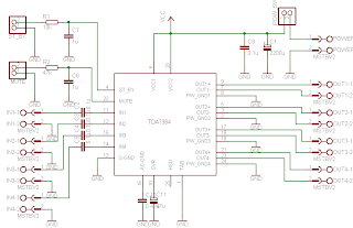

I didn’t find much information about this chip on the internet so I decided to built it and try on my own. As datasheets of TDA7384 says it is low distortion, low output noise, low external component count. Also has Stand-By function and Mute function. It has several protections like from output short circuit to GND or to Vs, capable to handle very inductive loads, thermal limiter, load dump voltage. TDA7384 is an AB power amplifier cased in flexiwatt25 (eagle library is included in project archive) package wich is designed for high end car radio applications. It allows rail to rail output voltage swing with no need of boot-strap capacitors.

Schematics TDA7384
Schematics TDA7384


I have followed the schematic in datasheed when building circuit. In datasheet you may also find PCB layout but it is two layered and didn’t fit to may box I’ve chosen. So I have made single sided PCB 50X100mm.


PCB TDA7384 amplifier

As I put pins on PCB for ST-BY and Mute but I not using them, I connected these pins to VCC like it is shown in PCB view. According to datasheet St-By and Mute turns off amplifier if signal in input is lower than 3.5V. So it is recommended to connect these pins to Vcc if not used.
Maximum power dissipation of chip is 80W(Tcase=70ºC), so it can handle 4 channels working at power of 20W each. But of course chip in a box doesn’t have good ventilation so I’ve put a radiator to ensure that amplifier effectively dissipates heats. I didn’t try to load amplifier to maximum to se if it doesn’t heat up to much. But at normal sound level it stays warm what is normal.


On box amplifier
On box amplifier


Dont forget to put thermal paste between chip and radiator to ensure lower thermal resistance. And here we go – brand new power amplifier ready to go:


TDA7384 Already to use
Already to use


source: [link]

Readmore → TDA7384 4 x 22W car power amplifier

Wednesday, 25 January 2017

Power amplifier circuit 60 W mono


Wow this is nice intregated amplifier circuit , because this IC can be power output up to 60 Watt . With minimum require voltage 8 V , and maximum voltage 35 V . But this circuit is'nt so good to working on car , because output sound is very loud but not smooth. Amplifier so good working on full range , with speaker full range 100W and impedance 8 Ohm.
Below it is schematic :


Click to view large

The circuit above use IC AN7170 , the original output power IC is 20 W with impedance. But with use the circuit output elevated up to 60W.

Readmore → Power amplifier circuit 60 W mono

Tuesday, 24 January 2017

LM1875 20 Watt Audio Power Amplifier


20 Watt amplifier
20 Watts Power Amplifier circuit can be made ​​with an IC power amplifier LM1875. IC LM1875 is a single chip power amplifier from National. 20 watts audio amplifier with LM1875 is a low power amplifier with good quality to the room.


To assemble the amplifier 20 watts with IC LM1875 component is not needed much support. 20 watts power amplifier using LM1875 IC in this article using symmetrical power supply. The virvuit of 20 watts audio power amplifier with IC LM1875 can be used as an experiment or first project for the reader, because it is simple and assembly of high success.

LM1875 | 20 Watt Audio Power Amplifier
Schematic Amplifier LM1875

LM1875 amplifier circuit with the above may result in the strengthening of the voltage up to 27dB for each channel (1 channel 1 IC). Strengthening the voltage can be changed by changing the feedback that is R5 R (on the circuit above using R 22K). But the tension reinforcement can not be less than 20 dB because it can cause oscillation. For the power supply or power supply 20 watts power amplifier rngakaian with lm1875 can use travo 2-3A with CT.

Readmore → LM1875 20 Watt Audio Power Amplifier

Sunday, 22 January 2017

zBot 10 A Power Stage for DC Motor Circuit Diagram


zBot :10-A Power Stage for DC Motor Circuit Diagram . If you look at the chassis of the zBot vehicle1, you’ll find two parts requiring intelligent control: the steering servo and the DC motor. The so called H-bridge is the normal circuit for electronic control of revolution speed and direction. The DC motor of a Tamiya car is powerful enough to propel zBot at up to 20 miles per hour.
.
The motor then consumes more than 10 A, so we choose high-current power MOSFETs for the driver stage. There are lots of different devices to choose from. The MOSFET we require has to supply the maximum motor current and, importantly, it has to be switched with gate voltages of about 5 V. In this case, the microcontroller switches the power stage (‘low side’) directly. For high side driving level shifters are necessary. The schematic of the H-bridge power stage shows a few inverters, NAND gates and two tri-stateable drivers. These logic functions are very important as the easier way, i.e.., directly controlling all four MOSFET has a fatal disadvantage.

zBot :10-A Power Stage for DC Motor Circuit Diagram

zBot :10-A Power Stage for DC Motor Circuit Diagram


In case of a software crash it could happen that two ore more MOSFETs are switched on incor-rectly for exam-ple, T4 and T7. In that case, the current through the transistors is limited by the internal resistors of the MOSFETs (about 10 mO) only. Such a fatal error would destroy the MOSFETs. The logic functions configured here effectively avoid illegal states.To control the DC motor, three signals are needed: DIR, PWM and STOP. DIR controls the direction of the motor revolution, PWM the speed, and STOP brakes the motor.

The software module for the DC motor is called dcm.c.(070172-I) The complete document called Zbot  the Robot Experimental Platform is available for free downloading from the Elektor Electronics website. The file number is 070172-11.zip (July/August 2007).

Sourced by : Circuitsstream.blogspot.com

Readmore → zBot 10 A Power Stage for DC Motor Circuit Diagram

Friday, 20 January 2017

Variable DC Power Supply Rise Circuit Diagram


This Variable DC Power Supply (Rise) Circuit Diagram project provides the schematic & the parts list needed to construct a simple DC Power Supply from an input power supply of 7-20 V AC or 7-30V DC. This project will come in handy in case you use plenty of batteries for your basic electronics project.

Two DC voltage outputs are available; is a fixed regulated 5V for TTL use. The other output is variable from 5V upwards. The maximum output voltage depends on the input voltage. The specified maximum input DC voltage to the regulator is 35V. The maximum input voltage must be two volts higher than the regulated output voltage.

 Variable DC Power Supply (Rise) Circuit Diagram
Variable DC Power Supply Circuit Diagram


The DC Power Supply circuit is based around the 7805 voltage regulator. It's only three connections input, output & ground & it provides a fixed output. The last digits of the part number specify the output voltage, e g. 05, 06, 08, ten, 12,15, 18, or 24. The 7800 series provides up to one amp load current & has on-chip circuitry to close down the regulator if any attempt is made to operate it outside its safe operating area.It can be seen that there's in fact separate circuits in this power supply. 7805 is directly connected as a fixed 5V regulator. The second 7805 has a resistor divider network on the output. A variable 500 ohm potentiometer is used to vary the output voltage from a maximum of 5V up to the maximum DC voltage depending on the input voltage. It will be about 2V below the input DC voltage.

The capacitor across the output improves transient response. The giant capacitor across the input is a filter capacitor to help smooth out ripple in the rectified AC voltage. The larger the filter capacitor the lower the ripple.

For tiny applications the heat sinks won't be needed. The tab on the regulator will dissipate 2W at 25 o C in air. (This is equivalent, for example, to an input voltage of 9V, an output of 5V & drawing 500 m A.) However, as your projects get bigger they will draw more current from the power supply and the regulators will operate at a higher temperature and a heat sink will be needed. You can basically add voltage & current meters to it and put it in to an appropriate plastic case connected to a transformer.

Trouble Shooting Procedure

An LED has been put in to the output of the fixed 5V regulator to indicate that the circuit is working. Poor soldering is the most likely reason that the circuit does not work. Check that all the soldering is done properly. Check that all parts are in their correct position on the PCB. Other items to check are to make sure that the regulators, electrolytic capacitor & bridge rectifier are inserted in the correct orientation.

Readmore → Variable DC Power Supply Rise Circuit Diagram