Showing posts with label amplifier. Show all posts
Showing posts with label amplifier. Show all posts
Wednesday, 15 February 2017
Audio amplifier circuit with IC STK0039 good quality amplifier

Although the output of which was issued in this circuit only 35watts maximum, but th esound can be issued harsh , loud , and clear. If the voltage is fit and clean , how to assembly , components are good , the right speakers , this circuit will definitely make a sound that good to hear the ear.
See audio amplifier circuit below :

Technical Information :Vcc Max = 45VVcc TYP = 30VPo = 35WRL = 8OhmIcco TYP = 40mAIcco Max = 80mAI Max = 10A

The amplifier can use to : tuner , subwoofer surround amplifier , surround amplifier , subwoofer system , car amplifier , PC amplifier , DVD/CD amplifier , Room amplifier . Because this amplifier good quality amplifier circuit.


Wednesday, 1 February 2017
3 4 W power amplifier schematic
The schematic above is amplifier based on ic TA7211P or TA7212P , circuit above using OT transformer as a booster amplifier again. The amplifier suitable used on outside / field, because by using a transformer OT is identical to the PA amplifier.

Part List :R = 1K , 10R , 3K3C = 1uF , 10uF , 1n , 68u, 3u3, 2n2 x 2, 100uIC = TA 7211P / TA7212PTechnical information :Max Vcc = 15 VDCMin Vcc = 4 VDCPo = 3,4 WRl = 8 OhmIcco = 16 mA
Sunday, 15 January 2017
IC LM12 150 Watts high power amplifier
To supply the required voltage to the amplifier circuit minimum of 7 Volt and a maximum of 24 volts . Incurred sizable ouput for amplifier ic 300 W maximum output.

R1_____________________________________10K
R2_____________________________________10K
R3_____________________________________220K
R4_____________________________________2.2R 2W
C1_____________________________________1uF
C2_____________________________________1000uF
C3_____________________________________68pF
D1_____________________________________BY229
D2_____________________________________BY229
L1_____________________________________4MH
IC1____________________________________LM12
Thursday, 12 January 2017
6 Watt stereo power amplifier schematic
Basiccally,this amplifier works with the IC, which is where ic is associated with several other components in the supply and use DC voltage, which corresponds to the needs of IC above course on the circuit schematic. For IC , stands intregated circuit used is ic LM379 which has a maximum 6 Watt stereo output. This IC manufactered by NS and with SDIP-14 package. While other components needed in the circuit schematic , you can see components of the list below.

Resistor
R1___________________2K
R2___________________2K
R3___________________33K
R4___________________33K
R5___________________1M
R6___________________1M
R7___________________10R 2W
R8___________________10R 2W
Capacitor
C1___________________4.7uF
C2___________________4.7uF
C3___________________470uF
C4___________________470uF
C5___________________470uF
C6___________________100n
C7___________________100n
IC
IC1___________________LM379
Friday, 6 January 2017
24 W BTL or 2 x 12 watt stereo amplifier
GENERAL DESCRIPTION:
The TDA1518BQ is an integrated class-B output amplifier in a 13-lead single-in-line (SIL) plastic power package. The device is primarily developed for car radio applications.
FEATURES:
- Requires very few external components
- Flexibility in use stereo as well as mono BTL
- High output power (without bootstrap)
- Low offset voltage at output (important for BTL)
- Fixed gain
- Good ripple rejection
- Mute/stand-by switch
- Load dump protection
- A.C. and d.c. short-circuit-safe to ground and VP
- Thermally protected
- Reverse polarity safe
- Capability to handle high energy on outputs (VP = 0 V)
- No switch-on/switch-off plop
- Flexible leads
- Low thermal resistance
- Identical inputs (inverting and non-inverting)
- Compatible with TDA1516BQ (except gain).
Circuit diagram:
 |
| Circuit diagram for mono amplifier TDA1518 |
 |
| Circuit diagram for stereo amplifier TDA1518 |
Datasheet for TDA1518: Download
Thursday, 5 January 2017
6 12 Volt audio amplifier circuits

The above is an amplifier circuit using supply voltages from 6 volts DC to 12 Volt DC. Power output of the amplifier is quite low with only 1 Watt 8 ohm impedance. You can apply this to the audio signal amplifiers that require strengthening are not so large as in the pocket radio.Part List :
R1 = 100K
R2 = 39R
R3 = 100R
C1 = 100nF
C2 = 100uF
C3 = 100uF
C4 = 100uF
C5 = 470uF
C6 = 100nF
C7 = 68pF
C8 = 1nF
C9 = 47uF
IC = SFC2790C
Friday, 30 December 2016
Stereo TDA2822 audio power amplifier circuit

In this series I use IC tda2822M as the main amplifier, but if you want to use in addition to IC TDA2822M you can use ic I mentioned this is KA2209, NJM2073, U2822B, U2823B. Output is issued no more than 4W, which had low output. Supply voltage from 3 volts to 16 volts.
Below its schematics of TDA2822 stereo audio power amplifier
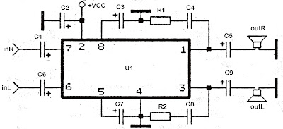
R1 = 4.7R
R2 = 4.7R
C1 = 1uF
C2 = 100uF
C3 = 100uF
C4 = 0.1uF
C5 = 470uF
C6 = 1uF
C7 = 100uF
C8 = 0.1uF
C7 = 100uF
C8 = 0.1uF
C9 = 470uF
ICs = KA2209 , NJM2073 , TDA2822 , U2822B , U2823B
Tuesday, 27 December 2016
Booster amplifier circuit
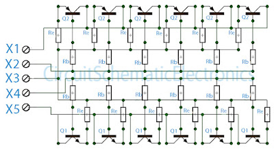
The above circuit is a circuit of booster amplifiers or amplifier end of a power amplifier circuit, Circuit over in the most important influence whether or not , and many more are affected in this final series. Because the booster circuit is the amplifier end of the work was too heavy components causing the rapid component of the heat. If we are wrong then consequences will install components that can cause fatal damaged direct component , such us the installation of pin emiter, collector , and base everything must be correct. In the circuit above can strengthen booster amplifier with maximum work and everything is evenly split, what is it evenly split ? evenly split the point here is that all components can work with the same voltage and the heat evenly , this is because at each respetive base transistor were given the same constrains and same wattage resistor. And to maintain if the power output is too large then the resistor on Re will hamper so that the transistor is not easily broken.
Part List :
Rb=10R/1W
Re=0,5-1R/5W
Q1=Transistor power NPN such us 2N3055 , TIP3055,TIP120,TIP142,2SC2922 , etc.
Q2=Transistor Power PNP such us MJ2955 ,TIP2955,TIP125,TIP147,2SA1216, etc.
X1=Voltage connector (-)
X2=PNP Base connector
X3=Speaker connecor but also must be connected from the buffer
X4=NPN base connector
X5=Voltage connector (+)
Wednesday, 14 December 2016
1400W audio power amplifier

This is an amplifier circuit that has a high output power is 1400W mono, the audio amplifier circuit is very suitable when used in a large room, using a woofer speaker, and fullrange. To sound out very nice, loud sound and almost no noise.
The amplifier using a transistor amplifier-quality, and for the final amplifier transistors can use a variety of high-power transistors. Minimum required supply voltage + / - 25V and a maximum of up to + /-90V.

For transistor 11 to 17 should use a heatsink, because if the maximum working range of the transistor heat and should be to install the heatsink. But do not forget also to the final amplifier transistor circuit should also be given a heatsink such as transistors 18 to 21.
Part List :
Resistor
R1_____560Ω
R2_____100Ω
R3_____2K2Ω
R4_____560Ω
R5_____1Ω
R6_____27KΩ
R7_____10KΩ
R8_____100Ω
R9_____100Ω
R10____100Ω
R11____12KΩ
R12____100Ω
R13____100Ω
R14____100Ω
R15____27KΩ
R16____2K2Ω
R17____560Ω
R18____100Ω
R19____10KΩ
R20____330Ω
R21____47Ω 2W
R22____56Ω
R23____2K2Ω
R24____22Ω
R25____56Ω
R26____180Ω
R27____500-1KΩ Trim
R28____560Ω
R29____56Ω
R30____56Ω
R31____22Ω 1W
R32____5Ω6 2W
R33____10Ω
R34____180Ω
R35____100Ω
R36____22Ω 2W
R37____180Ω
R38____56Ω
R39____47Ω 2W
R40____5Ω6 2W
R41____10Ω
R42____10Ω
R43____10Ω
R45____10Ω
R46____0.22Ω 5W
R47____0.22Ω 5W
R48____0.22Ω 5W
R49____0.22Ω 5W
R50____10Ω 5W
Capacitor
C1_____1цF
C2_____1.5nF
C3_____0.1цF 250-275V
C4_____0.1цF 250-275VC5_____100nF
C6_____100цF 50V
C7_____39pF
C8_____330pF
C9_____330pF
C10____330pF
C11____47nF 250-275V
C12____220nF 250-275V
Transistor
T1_____MJE340
T2_____2N5551 / C2240
T3_____2N5551 / C2240
T4_____2N5551 / C2240
T5_____2N5551 / C2240
T6_____2N5401 / BF423
T7_____2N5401 / BF423
T8_____2N5401 / BF423
T9_____2N5401 / BF423
T10____MJE350
T11____B1186
T12____TIP127
T13____D1763
T14____D1763
T15____B1186
T16____C5198
T17____A1941
T18____2SC2922 / MJ15024G
T19____2SC2922 / MJ15024G
T20____2SA1216 / MJ15025G
T21____2SA1216 / MJ15025G
Saturday, 10 December 2016
TDA8560Q Audio amplifier 2x40W

TDA8560Q general description:
TDA8560Q general description:
Unfortunately, some of the proposed scheme in the network and even a scheme recommended by the developer (Philips), fail to achieve the desired result. As an example of how not to suggest that you include the TDA8560 material published on Online Soldering: Car Amplifier 2x40 Watt (I should note that everything except the input circuits and the number of points on diet, still deserves attention). the initial inclusion of IMS (at power up, the load is connected and there is no input signal) can throw you into a state of perplexity / mild shock (it depends on the degree of hope is for your TDA). Chip is unstable, there are noises when the input signal is amplified last weakly and passed with distortions. IC bypass surgery fixed resistor at the input, the other measures in consultation with the source device does not help. Why and what to do? Really caught Palen chip and will have to buy a new one? Not so fast! The fact that Philips did not include measures to prevent the self-excitation of the IC, but I think they know about it, but do not tell anyone (not good, gentlemen!) Rid chip excitement can (and should) in a way that is not described here. This is so far, my little secret. Usually TDA8560 include approximately recommend the following scheme: TDA8560Q Audio amplifier 2x40W
TDA8560Q Features:
- Supply voltage: 6 - 18; typical 14.4 V.
- The peak output current: 7.5 A.
- The current in idle mode: 120 mA.
- Long-term power output, with
- RL = 4 ohms, THD = 10%, F = 1 kHz, 25 W,
- RL = 2 ohms, THD = 10%, F = 1kHz: 40W.
- Voltage gain, Au: 40 dB.
- Input Impedance: 30 ohms.
- Input Sensitivity: 100 mV.
- Frequency response: 20 - 20000 Hz.
- Requires very few external components
- High output power
- Low output offset voltage
- Fixed gain
- Diagnostic facility (distortion, short-circuit and temperature detection)
- Good ripple rejection
- Mode select switch (operating, mute and standby)
- Load dump protection
- Short-circuit safe to ground, to VP and across the load
- Low power dissipation in any short-circuit condition
- Thermally protected
- Reverse polarity safe
- Electrostatic discharge protection
- No switch-on/switch-off plop
- Flexible leads
- Low thermal resistance.
TDA8560Q amplifier diagram, circuit:
 |
| TDA8560Q amplifier diagram, circuit |
TDA8560Q layout:
 |
| TDA8560Q amplifier Layout |
 |
| TDA8560Q amplifier pcb |
Datasheet for TDA8560Q: Download
Friday, 2 December 2016
2 X 0 6W schematic audio amplifier
This schematic have require minimum voltage at 1Volt and maximum volotage at 9 Volt. Maximum output power 2 X 0.6W.

Part List:
Capacitor
C1 = 100uF
C2 = 220uF
C3 = 220uF
C4 = 220uF
C5 = 220uF
IC = ULN3782
Tuesday, 29 November 2016
Headset amplifier via USB
Headset amplifier via USB circuit is a series that is used to add a gain on the headset, which is used on a computer headset. Indeed not only on a computer course in all the headset could also, but in the above circuit voltage to utilize voltage mensupply issued on a PC or laptop via USB. So you need not bother looking for supply voltage, you just take it from USB.
 Part List :
Resistor
R1 = 20K
R2 = 10K
R3 = 10K
Capacitor
C1 = 3u3F 50V
C2 = 100pF
Diode
D1 = 1N4148
D2 = 1N4148
D3 = 1N4148
D4 = 1N4148
IC
U1 = JRC4558
Connector X1
1 = Output
2 = Input
3 = Ground
Connector X2
1 = V+ 5V from USB
2 = Ground From USB
Resistor
R1 = 20K
R2 = 10K
R3 = 10K
Capacitor
C1 = 3u3F 50V
C2 = 100pF
Diode
D1 = 1N4148
D2 = 1N4148
D3 = 1N4148
D4 = 1N4148
IC
U1 = JRC4558
Connector X1
1 = Output
2 = Input
3 = Ground
Connector X2
1 = V+ 5V from USB
2 = Ground From USB
 |
| PCB design Views |
Subscribe to:
Posts (Atom)