Showing posts with label IC. Show all posts
Showing posts with label IC. Show all posts
Wednesday, 15 March 2017
Adjustable Voltage Current Power Supply Circuit Using IC L200
IC2 is connected as a differential amplifier and compares the signals at its two inputs.
Referring to the circuit diagram: the input comprises a mains switch, fuse, transformer, bridge rectifier and smoothing capacitor (C2).
The difference between the inputs is the voltage drop across 'current’ sensor R4. This IC feeds the current sensing input (pin 2) of the L200.
P1 in the feedback loop of the 741 is used to vary the output current of the circuit. IC1 must be mounted on a suitable heat sink as it dissipates nearly all the power of the circuit.
The reference level output from I pin 4 of IC1 goes to the voltage divider made up of R5 and P2 (this pot sets the value of the output voltage).
The power supply can quite easily be built into a case and a voltmeter and ammeter mounted on the front panel. ln view of the accuracy of the circuit these should ideally be digital meters, but virtually any type will do.
If you compare the expense and the rating of this power supply you will get a surprise, because the output voltage and current are fully adjustable between O. . . 18 V and 0 . . . 1.8 A respectively and costs have still been kept very reasonable.
Diode D5 and capacitor C1 produce a negative auxiliary voltage, which is stabilized by zener diode D6 and capacitor C4.
All this is necessary to enable the output voltage to be adjusted down to zero volts. During the construction of this part of the circuit bear in mind that the positive lead of electrolytic capacitor C4 is connected to earth! Regulation is provided by IC1 and IC2. Capacitor C3 suppresses any residual transients at the input of lC1 and it should therefore be connected as closely as possible to IC1 similarly C4 and IC2).
The negative voltage provides the negative supply for the two ICs.


Sunday, 12 March 2017
Simple Surround audio amplifier circuit based on the IC TDA7053
Perhaps the surround amplifier circuit below is an interesting circuit is made. For, making easy just by using the IC and electrolytic capacitor added 1 , we already can hear the strains of music with sound ( Front Left ,Right and surround Right , Left. In addition to listening to music , this amplifier is also very suitable for gamers who want good sound quality.

Minimum voltage requred 9 volts and maximum of 15 volts. Power Output of each speaker 10 Watt with 4 ohm impedance.
Friday, 3 March 2017
Simle DC to AC Inverter by IC 555
This be basic AC inverter Circuit. Convenient for the initiator who have to is extremely fond of something experience. Because of use IC 555 highly popular, perform produce the frequency ,then enlarge with transistor NPN and PNP number TIP41 and TIP42 drive the coil transformer. Get by can pay Voltage output about 120V to 230V at frequency 50Hz. By have R4 perform control the frequency and should use. Voltage supply about 5V to 15V the detail sees in circuit picture sir.
Simple DC to AC Inverter by IC 555 Circuit Diagram

Thursday, 2 March 2017
Single IC Dual tones Siren Circuits Diagram
Double-tone Police sound Circuits Diagram
This circuit is intended for children fun, and can be installed on bicycles, battery powered cars and motorcycles, but also on models and various games and toys. With SW1 positioned as shown in the circuit diagram, the typical dual-tone sound of Police or Fire-brigade cars is generated, by the oscillation of IC1A and IC1B gates. With SW1 set to the other position, the old siren sound increasing in frequency and then slowly decreasing is reproduced, by pushing on P1 that starts oscillation in IC1C and IC1D.
The loudspeaker, driven by Q1, should be of reasonable dimensions and well encased, in order to obtain a more realistic and louder output. Tone and period of the sound oscillations can be varied by changing the values of C1, C2, C5, C6 and/or associated resistors. No power switch is required: leave SW1 in the low position (old-type siren) and the circuit consumption will be negligible.
Single -IC Dual-tones Siren Circuits Diagram

Parts:
R1,R3___470K 1/4W Resistors
R2______680K 1/4W ResistorR4_______82K 1/4W ResistorR5______330K 1/4W ResistorR6_______10K 1/4W ResistorR7_______33K 1/4W ResistorR8________3M3 1/4W ResistorC1,C5_____10µF 25V Electrolytic Capacitors
C2,C6_____10nF 63V Polyester Capacitors
C3_______100nF 63V Polyester CapacitorC4_______100µF 25V Electrolytic CapacitorD1-D3___1N4148 75V 150mA Diodes IC1_____4093 Quad 2 input Schmitt NAND Gate ICQ1______BC337 45V 800mA NPN Transistor P1______SPST Pushbutton
SW1_____DPDT Switch
SPKR____8 Ohm Loudspeaker
B1______6V Battery (4 AA 1.5V Cells in series)
Thursday, 16 February 2017
Simple LED flasher circuit using NE555 timer IC
This circuit consumes more power, but it's advantage is when you need a variable flash rate, like for strobe circuits. You can actually use this circuit as a remote control for strobes that have a remote input. Of course, it has many other applications besides strobes.

- R1, R2, C1 and the supply voltage determine the flash rate. Using a regulated power supply will do much to insure a stable flash rate. For a variable flash rate, replace R1 with a 1 megohm pot in series with a 22k resistor.
- The duty cycle of the circuit (the percentage of the time LED 1 is on to the time it is off during each cycle) is deterimed by the ratio of R1 to R2. If the value of R1 is low in relationship to R2, the duty cycle will be near 50 percent. If you use both LEDs, you will probably want a 50 percent duty cycle. On the other hand, if R2 is low compared to R1, the duty cycle will be less than 50 percent. This is useful to conserve battery life, or to produce a strobe type effect, when only LED1 is used.
- The NE555 timer chip can be damaged by reverse polarity voltage being applied to it. You can make the circuit goof proof by placing a diode in series with one of the supply leads.
- The purpose of R3 and R4 is to limit current through the LEDs to the maximum they can handle (usually 20 milliamps). You should select the value of these according to the supply voltage. 470 ohms works well with a supply voltage of 9-12 volts. You will need to reduce the value for lower supply voltages.
- Rainbow Kits offers several kits to build the above circuit. You can also order these kits from RadioShack.com. The Radio Shack catalog numbers (and web pages) are as follows: standard kit with two 5mm red LEDs, (990-0067), kit with two red, two green and two yellow 3mm LEDs, (990-0063), kit with jumbo green LEDs, (990-0048), kit with jumbo red LEDs, (990-0049). You can also buy all the parts to build the circuit at your local Radio Shack store, including a circuit board (276-159B).
I have built a miniature strobe circuit as follows. Use a 250k pot in series with a 4.7k resistor for R1. The 4.7k resistor sets the upper flash rate limit. Use 2.2k for R2. That sets a really short duty cycle. For this circuit, you don't use LED 2 or R4. For LED 1, I used a two Radio Shack white LEDs in series and no R-3. The circuit runs on a 9 v battery. link
Wednesday, 15 February 2017
Audio amplifier circuit with IC STK0039 good quality amplifier

Although the output of which was issued in this circuit only 35watts maximum, but th esound can be issued harsh , loud , and clear. If the voltage is fit and clean , how to assembly , components are good , the right speakers , this circuit will definitely make a sound that good to hear the ear.
See audio amplifier circuit below :

Technical Information :Vcc Max = 45VVcc TYP = 30VPo = 35WRL = 8OhmIcco TYP = 40mAIcco Max = 80mAI Max = 10A

The amplifier can use to : tuner , subwoofer surround amplifier , surround amplifier , subwoofer system , car amplifier , PC amplifier , DVD/CD amplifier , Room amplifier . Because this amplifier good quality amplifier circuit.

Thursday, 2 February 2017
Simple IC 555 Timer Tester Circuit Diagram
This is a Simple IC 555 Timer Tester Circuit Diagram. This simple and easy-to-use gadget not only tests the IC 555 timer in all its basic configurations but also tests the functionality of each pin of the timer. Once a timer is declared fit by this gadget, it will function satisfactorily in whatever mode or configuration you may try it. The two basic configurations in which a timer IC 555 can be used are the astable and the monostable modes of operation.
When the DPDT switch (S2) is in position 1-1, the timer under test automatically gets wired as a monostable multivibrator. In this case, the monoshot can be triggered by the microswitch (S1). The debouncing circuit constituted by the two NAND gates of IC1 (N1 and N2) produces a clean rectangular pulse when the microswitch is pressed. Resistor R3, capacitor C1 and diode D1 ensure that the trigger terminal of timer IC 555 (pin 2 is the trigger terminal) gets the desired positive-to-ground trigger pulse. This differentiator circuit also ensures that the width of the trigger pulse is less than the expected monoshot output pulse.
Simple IC 555 Timer Tester Circuit Diagram

The monoshot output pulse width is a function of the series combination of resistor R8 and potentiometer VR2, and capacitor C4. When DPDT switch S2 is in position 2-2, the timer gets configured for the astable mode of operation. The output is a pulse train with the high time period determined by the series combination of resistors R8, potentiometer VR2, resistor R9 and capacitor C4, whereas the low time period is determined by resistor R9 and capacitor C4.
The reset terminal of timer IC (pin 4) should be tied to Vcc normally. More precisely, the voltage at pin 4 should be greater than 0.8V. A voltage less than that resets the output. Whether you have connected the timer in the monoshot or astable mode of operation, the output goes low the moment you bring the reset terminal below 0.8V.
The control terminal (pin 5) can be used to change the high time (‘on’ time) of the output pulse train in the astable mode and the output pulse width in the monoshot mode by applying an external voltage. This external voltage basically changes the reference voltage levels of the comparators inside the IC. The levels are set by three identical resistors of usually 5 kilo-ohms inside the IC connected from Vcc to ground, at 2/3Vcc for pin 5 and 1/3Vcc for pin 2. These levels can be changed by connecting an external resistor between pin 5 and ground. Resistor R10 and potentiometer VR3 have been connected for this purpose.
The pulse width in the monoshotmode is given by:
1.1×total charging resistance×charging capacitance
This expression is valid when there is no external resistor connected at pin 5. The pulse width can be reduced by connecting an external resistor.
The high and low time periods in the astable mode are:
High time period = 0.69×chargingresistance×charging capacitance
Low time period = 0.69×dischargeresistance×capacitance
Again the expressions are true with no external resistor at pin 5. The high time period can be made to decrease by connecting an external resistor between pin 5 and ground.
The circuit can thus be used to check:
1. The timer IC in astable configuration.
2. The timer IC in monostable configuration.
3. The capability of the reset terminal to override all functions and rest the output to low.
4. The function of the control terminal to change the ‘on’ or the ‘high’ time of the output waveform in astable mode of operation and the output pulse width in monostable mode of operation.
The circuit operates off a 9V battery, which makes the gadget portable. You can construct it easily on any general-purpose PCB along with the 8-pin socket.
To test an IC 555:
1. Insert it into the socket.
2. Set switch S2 in position 1-1.
3. Switch on the power supply by flipping switch S3 to ‘on’ position. Power-indicator LED (LED3) glows to indicate that the circuit is ready to test the IC timer.
4. If the IC is okay, LED1 glows because the IC is wired as a monoshot and in the absence of any trigger, its output is low.
5. Apply the trigger pulse by momentarily pressing switch S1. LED1 stops glowing and, in turn, LED2 glows. This confirms that the output of the monoshot has gone high. After the predetermined time period, LED2 goes off and LED1 again glows. Vary preset VR2 and trigger the monoshot again through switch S1. You will find that LED2 glows this time for a longer or a smaller time period depending upon whether you increased or decreased VR2 resistance.
6. For checking the reset function of the timer, trigger the monoshot again, and before the expected time is over, quickly decrease the potmeter VR1 resistance so as to bring the voltage at pin 4 below 0.8V. You will observe the output going low (indicated by glowing LED1 and extinguished LED2).
7. For checking the control function of the timer IC, set potmeter VR1 again in the maximum resistance position. Also set preset VR3 in the minimum resistance position. Trigger the monoshot using switch S1. You’ll observe its output going high for a time period that is much less than that determined from the series combination of R8 and VR2, and capacitor C4. In fact, for any fixed setting of this series combination, the output pulse width can be observed to vary for different values of potmeter VR3 resistance—by triggering the monoshot several times, once for each setting of VR3.
8. Now set the DPDT switch in position 2-2. LED1 and LED2 glow alternatively with the timing determined by the resistances in the charge and discharge paths. This means the timer IC is okay and wired in astable mode.
9. The functions of reset and control pins can be checked in astable configuration too in the same way as discussed above for the monoshot configuration.
The reset terminal of timer IC (pin 4) should be tied to Vcc normally. More precisely, the voltage at pin 4 should be greater than 0.8V. A voltage less than that resets the output. Whether you have connected the timer in the monoshot or astable mode of operation, the output goes low the moment you bring the reset terminal below 0.8V.
The control terminal (pin 5) can be used to change the high time (‘on’ time) of the output pulse train in the astable mode and the output pulse width in the monoshot mode by applying an external voltage. This external voltage basically changes the reference voltage levels of the comparators inside the IC. The levels are set by three identical resistors of usually 5 kilo-ohms inside the IC connected from Vcc to ground, at 2/3Vcc for pin 5 and 1/3Vcc for pin 2. These levels can be changed by connecting an external resistor between pin 5 and ground. Resistor R10 and potentiometer VR3 have been connected for this purpose.
The pulse width in the monoshotmode is given by:
1.1×total charging resistance×charging capacitance
This expression is valid when there is no external resistor connected at pin 5. The pulse width can be reduced by connecting an external resistor.
The high and low time periods in the astable mode are:
High time period = 0.69×chargingresistance×charging capacitance
Low time period = 0.69×dischargeresistance×capacitance
Again the expressions are true with no external resistor at pin 5. The high time period can be made to decrease by connecting an external resistor between pin 5 and ground.
The circuit can thus be used to check:
1. The timer IC in astable configuration.
2. The timer IC in monostable configuration.
3. The capability of the reset terminal to override all functions and rest the output to low.
4. The function of the control terminal to change the ‘on’ or the ‘high’ time of the output waveform in astable mode of operation and the output pulse width in monostable mode of operation.
The circuit operates off a 9V battery, which makes the gadget portable. You can construct it easily on any general-purpose PCB along with the 8-pin socket.
To test an IC 555:
1. Insert it into the socket.
2. Set switch S2 in position 1-1.
3. Switch on the power supply by flipping switch S3 to ‘on’ position. Power-indicator LED (LED3) glows to indicate that the circuit is ready to test the IC timer.
4. If the IC is okay, LED1 glows because the IC is wired as a monoshot and in the absence of any trigger, its output is low.
5. Apply the trigger pulse by momentarily pressing switch S1. LED1 stops glowing and, in turn, LED2 glows. This confirms that the output of the monoshot has gone high. After the predetermined time period, LED2 goes off and LED1 again glows. Vary preset VR2 and trigger the monoshot again through switch S1. You will find that LED2 glows this time for a longer or a smaller time period depending upon whether you increased or decreased VR2 resistance.
6. For checking the reset function of the timer, trigger the monoshot again, and before the expected time is over, quickly decrease the potmeter VR1 resistance so as to bring the voltage at pin 4 below 0.8V. You will observe the output going low (indicated by glowing LED1 and extinguished LED2).
7. For checking the control function of the timer IC, set potmeter VR1 again in the maximum resistance position. Also set preset VR3 in the minimum resistance position. Trigger the monoshot using switch S1. You’ll observe its output going high for a time period that is much less than that determined from the series combination of R8 and VR2, and capacitor C4. In fact, for any fixed setting of this series combination, the output pulse width can be observed to vary for different values of potmeter VR3 resistance—by triggering the monoshot several times, once for each setting of VR3.
8. Now set the DPDT switch in position 2-2. LED1 and LED2 glow alternatively with the timing determined by the resistances in the charge and discharge paths. This means the timer IC is okay and wired in astable mode.
9. The functions of reset and control pins can be checked in astable configuration too in the same way as discussed above for the monoshot configuration.
Sourced By: EFY. Author: Raj K. Gorkhali
Sunday, 15 January 2017
Advantages Disadvantages of RTD Thermocouple Thermistor Temp IC Sensors
Hi Greeting,
Friends we always come across various temperature sensors like RTD, Thermocouple, Thermistor, temperature sensing IC’s while doing automation of process plants. It’s very essential to know about advantages & disadvantages of the entire sensors so that we can select them with ease.
So let’s start with Thermocouple.
Thermocouple:

Advantages of Thermocouple:
- Self Powered
- Simple
- Rugged
- Inexpensive
- Wide Variety
- Wide Temp Range
Disadvantages of Thermocouple:
- Non Linear
- Reference Required
- Low Voltage
- Least Stable
- Least Sensitive
RTD:

Advantages of RTD:
- Most Stable
- Most Accurate
- More Linear than Thermocouple
Disadvantages of RTD:
- Expensive
- Current Source Required
- Small ∆R
- Low absolute Resistance
- Self heating
Thermistor:

Advantages of Thermistor:
- High Output
- Fast
- Two wire ohms measurement.
Disadvantages of Thermistor:
- Non Linear
- Limited Temperature Range.
- Fragile
- Current Source required.
- Self heating
IC Sensors:

Advantages of IC Sensor:
- Highest Output.
- Inexpensive.
- Most linear.
Disadvantages of IC Sensor:
- T< 200C.
- Power supply required.
- Slow.
- Limited Configuration.
- Self heating
IC LM12 150 Watts high power amplifier
To supply the required voltage to the amplifier circuit minimum of 7 Volt and a maximum of 24 volts . Incurred sizable ouput for amplifier ic 300 W maximum output.

R1_____________________________________10K
R2_____________________________________10K
R3_____________________________________220K
R4_____________________________________2.2R 2W
C1_____________________________________1uF
C2_____________________________________1000uF
C3_____________________________________68pF
D1_____________________________________BY229
D2_____________________________________BY229
L1_____________________________________4MH
IC1____________________________________LM12
Saturday, 14 January 2017
High temperature protector with IC 3584
IC 3584 has thermal protection or voltage automatically shutdown when the temperature at IC exceed 150 degrees or more. You can operate this circuit at the transistor or IC heatsing, if a transistor or IC had exceeded the limit of the heat circuit automatically shutdown.How to use a thermal shutdown circuit above that is first given a circuit of voltage V+,V-,and ground , the given a voltage Vin to be created automatically shutdown if the temperature is high , and the output is inserted in the circuit of an amplifier or other. Then IC embedded in the heatsing or case, which if too hot will shutdown alone. If the circuit already decided voltage, the voltage will re-connect if the temperature returns to normal.

Saturday, 7 January 2017
Schematic Power Amplifier with IC AN7112
Schematic Circuit use the IC AN7112 with minimum voltage 4 Volt and maximum voltage 14 Volt. Recomeneded voltage is 9 Volt. Maximum output power 0,5 watt. This is low output power or mini amplifier sound. Impedance Speaker 8 Ohm and frequncy 40 Hz - 18 kHz. IC AN7112 has similarities with IC KA2212 , LA4140 , TA7313AP . PAckage of this IC is SIL - 9 and Manufactered by MATSUSHITA.
See Schematic power amplifier (figure 1.1) and Package IC (figure 1.0) below :
 | ||
Figure 1.1 Click Image to View Enlarge
|

Faster Battery Charger Circuit 6 12 Volt with IC LM308 and LM317
This circuit is quickly charging the battery . If you need a faster charger ,this circuit is recomended to you . And this charger is low temperature , the temperatur is 5 degree celcius. Input Voltage is 15 Volt DC , and Output voltage to charging 6 -12V and you can adjust by the D1 (see schematic). And adjust the D1 to 50 mV greater VZ than D2 (see schematic). Couple the D2 to battery. This circuit operating by IC LM308 and LM317 and any other components. And you can use this circuit to charging Accu 6 or 12 Volt , dry or wet and other battery .
See this Schematic Circuit below :

Friday, 30 December 2016
Dual 15 W BTL power IC for car audio
The AN7195Z is an audio power IC developed for the sound output of car audio (dual 15 W).
 |
| Dual 15 W BTL power IC for car audio |
Thursday, 29 December 2016
Schematic Audio Amplifier with IC AN7108
See this circuit below:
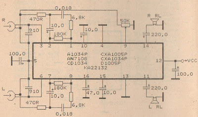
Datasheet IC AN7108
Vcc = 1-6,6 V
Pout = 2X 30 mW
RL = 32 Ohm
Ft = 20-20 Khz
Icco = 14 mA
Package = DIP-16
Manufactered = MATSUSHITA
Wednesday, 28 December 2016
DC to AC converter 12 to 100 Voltage circuit with IC
An AC-DC voltage converter with electrically isolated with onput and output circuits and converters with a transformer with at least one primary coil and a capacitor resonance said coil to at least one primary school.
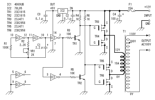
A switching transistor whose collector-emitter path is connected in series at least a coil and the primary school to the transistor switching system for the storage in the database of the surface sensors.
switching power transistor provides the foundation for the transistor switching system, and by other means in order to increase the voltage transmitter Collector of the transistor switching and deliver a response to such an increase and at least in the period immediately after the increase.
one while driving for the transistor circuit, the additional base current is very progressive with a predetermined, so that the storage of the relatively constant switching transistor in the beach for the operation of the converter.
Saturday, 24 December 2016
Compressor Circuit with 570 571 Compandor IC
Compressor Circuit with 570/571 Compandor IC circuit provide high gain for low amplitude input and provide low gain for high amplitude input. This action, in effect, produce a nearly constant amplitude even though the input has very high dynamic range (very high amplitude variation from time to time). The action of compression like this is needed in some situation, such as in maximizing modulation depth in broadcasting, or sustaining electric guitar signal which has very high variation between the plucking time and fading out. The following circuit has complementary input/output characteristic and unity gain at 0.775 VRMS input. Voltage gain through compressor is square root of 0.7/Vin. Vin is average input voltage. This circuit uses Signetics dual channel compandor IC. 570 has lower inherent distortion and higher supply voltage range (6-24 V) than 571 (6-18 V).
Compressor Circuit with 570/571

Source :circuitsdiagram-lab
Monday, 12 December 2016
Schematic Power Amplifier with IC TDA7370
Here..... this circuit is stereo power amplifier , based on IC TDA7370, its nice Intregated Power amplifier , He does not have hre slightest sound buzzing , although power amplifiers without additional reinforcement , such as filters , tone control, etc.

Voltage : 9 to 24 volts
Max. Power Output : 2 x 20 Watts
Impedance : 4 Ohms
Sunday, 11 December 2016
IC 555 Design Note Circuit Diagram
The popular Timer IC 555 is extensively used in short duration timing applications. IC 555 is a highly stable integrated circuit functioning as an accurate time delay generator and free running multivibrator. But one of the serious problem in 555 timer design is the false triggering of the circuit at power on or when voltage changes. The article describes how IC555 is designed perfectly to avoid false triggering.
555 IC pin functions
Pin1 Ground
Pin2 Trigger
Pin3 Output
Pin 4 Reset
Pin 5 Control voltage
Pin 6 Threshold
Pin 7 Discharge
Pin 8 Vcc
Functional aspects of pins
Trigger Pin 2
Usually pin2 of the IC is held high by a pull up resistor connected to Vcc. When a negative going pulse is applied to pin 2, the potential at pin 2 falls below 1/3 Vcc and the flip-flop switches on. This starts the timing cycle using the resistor and capacitor connected to pins 6 and 7.
Reset pin 4
Reset pin 4 can be controlled to reset the timing cycle. If pin 4 is grounded, IC will not be triggered. When pin4 becomes positive, IC becomes ready to start the timing cycle. Reset voltage is typically 0.7 volts and reset current 0.1 mA. In timer applications, reset pin should be connected to Vcc to get more than 0.7 volts.
Control Voltage pin 5
Pin5 can be used to control the working of IC by providing a DC voltage at pin5. This permits the control of the timing cycle manually or electronically. In monostable operation, the control pin5 is connected to ground through a 0.01 uF capacitor. This prevents the timing interval from being affected by AC or RF interference. In the Astable mode, by applying a variable DC voltage at pin 5 can change the output pulses to FM or PWM.
Threshold pin 6 and Discharge pin 7
These two inputs are used to connect the timing components- Resistor and Capacitor. The threshold comparator inside the IC is referenced at 2/3 Vcc and the trigger comparator is referenced at 1/3 Vcc. These two comparators control the internal Flip-Flop of the circuit to give High or Low output at pin 3.When a negative going pulse is applied to pin 2, the potential at pin2 drops below 1/3 Vcc and the trigger comparator switches on the Flip-Flop. This turns the output high. The timing comparator then charges through the timing resistor and the voltage in the timing capacitor increases to 2/3 Vcc.( The time delay depends on the value of the resistor and capacitor.
That is, higher values, higher time).When the voltage level in the capacitor increases above 2/3 Vcc, the threshold comparator resets the Flip-Flop and the output turns low. Capacitor then discharges through pin 7.Once triggered, the IC will not responds to further triggering until the timing cycle is completed. The time delay period is calculated using the formula T= 1.1 Ct Rt. Where Ct is the value of Capacitor in PF and Rt is the value of Resistor in Ohms. Time is in Seconds.
How to eliminate false triggering?
The circuit diagram shown below is the simple monostable using IC 555. To eliminate the false triggering resistor R1 and Capacitor C1 are connected to the reset pin 4 of the IC. So the reset pin is always high even if the supply voltage changes. Moreover capacitor C3 connected close to the Vcc pin 8 acts as a buffer to maintain stable supply voltage to pin 8. Using this design, it is easy to avoid false triggering to a certain extent.
555 IC pin functions
Pin1 Ground
Pin2 Trigger
Pin3 Output
Pin 4 Reset
Pin 5 Control voltage
Pin 6 Threshold
Pin 7 Discharge
Pin 8 Vcc
Functional aspects of pins
Trigger Pin 2
Usually pin2 of the IC is held high by a pull up resistor connected to Vcc. When a negative going pulse is applied to pin 2, the potential at pin 2 falls below 1/3 Vcc and the flip-flop switches on. This starts the timing cycle using the resistor and capacitor connected to pins 6 and 7.
Reset pin 4
Reset pin 4 can be controlled to reset the timing cycle. If pin 4 is grounded, IC will not be triggered. When pin4 becomes positive, IC becomes ready to start the timing cycle. Reset voltage is typically 0.7 volts and reset current 0.1 mA. In timer applications, reset pin should be connected to Vcc to get more than 0.7 volts.
Control Voltage pin 5
Pin5 can be used to control the working of IC by providing a DC voltage at pin5. This permits the control of the timing cycle manually or electronically. In monostable operation, the control pin5 is connected to ground through a 0.01 uF capacitor. This prevents the timing interval from being affected by AC or RF interference. In the Astable mode, by applying a variable DC voltage at pin 5 can change the output pulses to FM or PWM.
Threshold pin 6 and Discharge pin 7
These two inputs are used to connect the timing components- Resistor and Capacitor. The threshold comparator inside the IC is referenced at 2/3 Vcc and the trigger comparator is referenced at 1/3 Vcc. These two comparators control the internal Flip-Flop of the circuit to give High or Low output at pin 3.When a negative going pulse is applied to pin 2, the potential at pin2 drops below 1/3 Vcc and the trigger comparator switches on the Flip-Flop. This turns the output high. The timing comparator then charges through the timing resistor and the voltage in the timing capacitor increases to 2/3 Vcc.( The time delay depends on the value of the resistor and capacitor.
That is, higher values, higher time).When the voltage level in the capacitor increases above 2/3 Vcc, the threshold comparator resets the Flip-Flop and the output turns low. Capacitor then discharges through pin 7.Once triggered, the IC will not responds to further triggering until the timing cycle is completed. The time delay period is calculated using the formula T= 1.1 Ct Rt. Where Ct is the value of Capacitor in PF and Rt is the value of Resistor in Ohms. Time is in Seconds.
How to eliminate false triggering?
The circuit diagram shown below is the simple monostable using IC 555. To eliminate the false triggering resistor R1 and Capacitor C1 are connected to the reset pin 4 of the IC. So the reset pin is always high even if the supply voltage changes. Moreover capacitor C3 connected close to the Vcc pin 8 acts as a buffer to maintain stable supply voltage to pin 8. Using this design, it is easy to avoid false triggering to a certain extent.
555 Monostable circuit

A ready recknor to select timing resistor and capacitor

Theoretically long interval is possible with IC 555,but in practical conditions, it is difficult to get more than 3 minutes. If low leakage Tantalum capacitor is used, this can be increased to 5 minutes or more. If the value of the timing capacitor is too high above 470 uF, charging time will be prolonged which will upset the timing cycle and the output remains high even after the desired time is over.
Subscribe to:
Posts (Atom)