Showing posts with label 555. Show all posts
Showing posts with label 555. Show all posts
Friday, 3 March 2017
Simle DC to AC Inverter by IC 555
This be basic AC inverter Circuit. Convenient for the initiator who have to is extremely fond of something experience. Because of use IC 555 highly popular, perform produce the frequency ,then enlarge with transistor NPN and PNP number TIP41 and TIP42 drive the coil transformer. Get by can pay Voltage output about 120V to 230V at frequency 50Hz. By have R4 perform control the frequency and should use. Voltage supply about 5V to 15V the detail sees in circuit picture sir.
Simple DC to AC Inverter by IC 555 Circuit Diagram


Monday, 13 February 2017
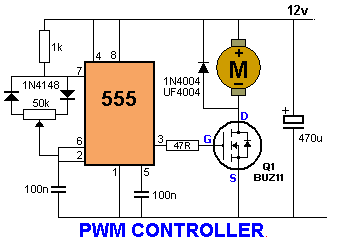
PWM Controller 555 timer circuits
Saturday, 4 February 2017
Auto Burglar Alarm Using 555 Timer ICs
This electronic circuit project using two 555 timer ICs, Simple circuit and low-cost circuit diagram, basic circuit could be used for a home also. The circuit Auto burglar alarm will sound your car horn if anyone opens the car door while the circuit is armed. The timers will allow you to leave the car without sounding the horn. To turn the circuit on S1 must be closed.
Auto Burglar Alarm Circuit Diagram:

To set the alarm, open S2 (it is normally closed ) this will give you about 5 seconds to get out and close the door. The exit delay time is set by R1 and C1. If anyone opens the doors for more than two seconds the horn will sound until power is removed from the circuit. The 2 second time is set by R2 and C2. If you open the door, you must deactivate the alarm by closing S2.
Auto Burglar Alarm Circuit Diagram:
To set the alarm, open S2 (it is normally closed ) this will give you about 5 seconds to get out and close the door. The exit delay time is set by R1 and C1. If anyone opens the doors for more than two seconds the horn will sound until power is removed from the circuit. The 2 second time is set by R2 and C2. If you open the door, you must deactivate the alarm by closing S2.
Thursday, 2 February 2017
Simple IC 555 Timer Tester Circuit Diagram
This is a Simple IC 555 Timer Tester Circuit Diagram. This simple and easy-to-use gadget not only tests the IC 555 timer in all its basic configurations but also tests the functionality of each pin of the timer. Once a timer is declared fit by this gadget, it will function satisfactorily in whatever mode or configuration you may try it. The two basic configurations in which a timer IC 555 can be used are the astable and the monostable modes of operation.
When the DPDT switch (S2) is in position 1-1, the timer under test automatically gets wired as a monostable multivibrator. In this case, the monoshot can be triggered by the microswitch (S1). The debouncing circuit constituted by the two NAND gates of IC1 (N1 and N2) produces a clean rectangular pulse when the microswitch is pressed. Resistor R3, capacitor C1 and diode D1 ensure that the trigger terminal of timer IC 555 (pin 2 is the trigger terminal) gets the desired positive-to-ground trigger pulse. This differentiator circuit also ensures that the width of the trigger pulse is less than the expected monoshot output pulse.
Simple IC 555 Timer Tester Circuit Diagram

The monoshot output pulse width is a function of the series combination of resistor R8 and potentiometer VR2, and capacitor C4. When DPDT switch S2 is in position 2-2, the timer gets configured for the astable mode of operation. The output is a pulse train with the high time period determined by the series combination of resistors R8, potentiometer VR2, resistor R9 and capacitor C4, whereas the low time period is determined by resistor R9 and capacitor C4.
The reset terminal of timer IC (pin 4) should be tied to Vcc normally. More precisely, the voltage at pin 4 should be greater than 0.8V. A voltage less than that resets the output. Whether you have connected the timer in the monoshot or astable mode of operation, the output goes low the moment you bring the reset terminal below 0.8V.
The control terminal (pin 5) can be used to change the high time (‘on’ time) of the output pulse train in the astable mode and the output pulse width in the monoshot mode by applying an external voltage. This external voltage basically changes the reference voltage levels of the comparators inside the IC. The levels are set by three identical resistors of usually 5 kilo-ohms inside the IC connected from Vcc to ground, at 2/3Vcc for pin 5 and 1/3Vcc for pin 2. These levels can be changed by connecting an external resistor between pin 5 and ground. Resistor R10 and potentiometer VR3 have been connected for this purpose.
The pulse width in the monoshotmode is given by:
1.1×total charging resistance×charging capacitance
This expression is valid when there is no external resistor connected at pin 5. The pulse width can be reduced by connecting an external resistor.
The high and low time periods in the astable mode are:
High time period = 0.69×chargingresistance×charging capacitance
Low time period = 0.69×dischargeresistance×capacitance
Again the expressions are true with no external resistor at pin 5. The high time period can be made to decrease by connecting an external resistor between pin 5 and ground.
The circuit can thus be used to check:
1. The timer IC in astable configuration.
2. The timer IC in monostable configuration.
3. The capability of the reset terminal to override all functions and rest the output to low.
4. The function of the control terminal to change the ‘on’ or the ‘high’ time of the output waveform in astable mode of operation and the output pulse width in monostable mode of operation.
The circuit operates off a 9V battery, which makes the gadget portable. You can construct it easily on any general-purpose PCB along with the 8-pin socket.
To test an IC 555:
1. Insert it into the socket.
2. Set switch S2 in position 1-1.
3. Switch on the power supply by flipping switch S3 to ‘on’ position. Power-indicator LED (LED3) glows to indicate that the circuit is ready to test the IC timer.
4. If the IC is okay, LED1 glows because the IC is wired as a monoshot and in the absence of any trigger, its output is low.
5. Apply the trigger pulse by momentarily pressing switch S1. LED1 stops glowing and, in turn, LED2 glows. This confirms that the output of the monoshot has gone high. After the predetermined time period, LED2 goes off and LED1 again glows. Vary preset VR2 and trigger the monoshot again through switch S1. You will find that LED2 glows this time for a longer or a smaller time period depending upon whether you increased or decreased VR2 resistance.
6. For checking the reset function of the timer, trigger the monoshot again, and before the expected time is over, quickly decrease the potmeter VR1 resistance so as to bring the voltage at pin 4 below 0.8V. You will observe the output going low (indicated by glowing LED1 and extinguished LED2).
7. For checking the control function of the timer IC, set potmeter VR1 again in the maximum resistance position. Also set preset VR3 in the minimum resistance position. Trigger the monoshot using switch S1. You’ll observe its output going high for a time period that is much less than that determined from the series combination of R8 and VR2, and capacitor C4. In fact, for any fixed setting of this series combination, the output pulse width can be observed to vary for different values of potmeter VR3 resistance—by triggering the monoshot several times, once for each setting of VR3.
8. Now set the DPDT switch in position 2-2. LED1 and LED2 glow alternatively with the timing determined by the resistances in the charge and discharge paths. This means the timer IC is okay and wired in astable mode.
9. The functions of reset and control pins can be checked in astable configuration too in the same way as discussed above for the monoshot configuration.
The reset terminal of timer IC (pin 4) should be tied to Vcc normally. More precisely, the voltage at pin 4 should be greater than 0.8V. A voltage less than that resets the output. Whether you have connected the timer in the monoshot or astable mode of operation, the output goes low the moment you bring the reset terminal below 0.8V.
The control terminal (pin 5) can be used to change the high time (‘on’ time) of the output pulse train in the astable mode and the output pulse width in the monoshot mode by applying an external voltage. This external voltage basically changes the reference voltage levels of the comparators inside the IC. The levels are set by three identical resistors of usually 5 kilo-ohms inside the IC connected from Vcc to ground, at 2/3Vcc for pin 5 and 1/3Vcc for pin 2. These levels can be changed by connecting an external resistor between pin 5 and ground. Resistor R10 and potentiometer VR3 have been connected for this purpose.
The pulse width in the monoshotmode is given by:
1.1×total charging resistance×charging capacitance
This expression is valid when there is no external resistor connected at pin 5. The pulse width can be reduced by connecting an external resistor.
The high and low time periods in the astable mode are:
High time period = 0.69×chargingresistance×charging capacitance
Low time period = 0.69×dischargeresistance×capacitance
Again the expressions are true with no external resistor at pin 5. The high time period can be made to decrease by connecting an external resistor between pin 5 and ground.
The circuit can thus be used to check:
1. The timer IC in astable configuration.
2. The timer IC in monostable configuration.
3. The capability of the reset terminal to override all functions and rest the output to low.
4. The function of the control terminal to change the ‘on’ or the ‘high’ time of the output waveform in astable mode of operation and the output pulse width in monostable mode of operation.
The circuit operates off a 9V battery, which makes the gadget portable. You can construct it easily on any general-purpose PCB along with the 8-pin socket.
To test an IC 555:
1. Insert it into the socket.
2. Set switch S2 in position 1-1.
3. Switch on the power supply by flipping switch S3 to ‘on’ position. Power-indicator LED (LED3) glows to indicate that the circuit is ready to test the IC timer.
4. If the IC is okay, LED1 glows because the IC is wired as a monoshot and in the absence of any trigger, its output is low.
5. Apply the trigger pulse by momentarily pressing switch S1. LED1 stops glowing and, in turn, LED2 glows. This confirms that the output of the monoshot has gone high. After the predetermined time period, LED2 goes off and LED1 again glows. Vary preset VR2 and trigger the monoshot again through switch S1. You will find that LED2 glows this time for a longer or a smaller time period depending upon whether you increased or decreased VR2 resistance.
6. For checking the reset function of the timer, trigger the monoshot again, and before the expected time is over, quickly decrease the potmeter VR1 resistance so as to bring the voltage at pin 4 below 0.8V. You will observe the output going low (indicated by glowing LED1 and extinguished LED2).
7. For checking the control function of the timer IC, set potmeter VR1 again in the maximum resistance position. Also set preset VR3 in the minimum resistance position. Trigger the monoshot using switch S1. You’ll observe its output going high for a time period that is much less than that determined from the series combination of R8 and VR2, and capacitor C4. In fact, for any fixed setting of this series combination, the output pulse width can be observed to vary for different values of potmeter VR3 resistance—by triggering the monoshot several times, once for each setting of VR3.
8. Now set the DPDT switch in position 2-2. LED1 and LED2 glow alternatively with the timing determined by the resistances in the charge and discharge paths. This means the timer IC is okay and wired in astable mode.
9. The functions of reset and control pins can be checked in astable configuration too in the same way as discussed above for the monoshot configuration.
Sourced By: EFY. Author: Raj K. Gorkhali
Friday, 20 January 2017
555 Tester Circuit Diagram

This is a Simple 555 Tester Circuit Diagram. The IC 555 is a widely used timers, control circuits, PWM, alarms, etc.. Often we set up a circuit that does not work or works differently than expected, this time the ideal is a test circuit for this IC.
This test circuit 555 is connected as an astable multivibrator when the button switch S1 is pressed, the LEDs D1 and D2 flash alternately. Ie, when the output is high D2 will light when the output is low D3 will light, and the other a Hi Lo. The speed of flashes is determined by the components R1, R2 and C1.Pressing the S1 test the 555 starts and any change in the IC flashes may consider to be defective.

Sunday, 15 January 2017
Build a Simple Home Alarm Circuit Using 555 ICs
This is a Simple Home Alarm Circuit Using 555 IC's. This circuit can be simplified by using a single 74C14 IC. This IC is also known by the following numbers: 40106, 40014, and 74HC14. These are CMOS chips and are characterised by low current consumption, high input impedance and a supply voltage from 5v to 15v. (Do not substitute 7414 or 74LS14. They are TTL chips and operate on 4.5v to 5.5v and have low impedance inputs.)
Simple Home Alarm Circuit Diagram

Simple Home Alarm Circuit Diagram
The 74C14 contains 6 Schmitt Trigger gates and 4 of these gates (Schmitt Inverters) are used in this circuit.
The circuit consists of a number of "building blocks" and the first consists of two transistors in a very clever "bootstrap" arrangement. The first transistor is turned on via the 3M3 and 47k. The second transistor is not turned on and the output is HIGH.
A small signal from the electret microphone will consist of positive and negative excursions and the negative excursion will turn the first transistor OFF. This will turn the second transistor ON and the left lead of the 100n will be pulled towards the 0v rail. The 100n is uncharged and the right lead will also be pulled towards the 0v rail and the input of the 74C14 will see a LOW. This will make the output HIGH and turn on the BC547 transistor.
When the second transistor turns ON, it also pulls the 2u2 down and this removes the "turn-on" voltage to the first transistor. The two transistors remain in this state for a few seconds while the 2u2 discharges and the voltage on the base of the first transistor rises. When this happens, the two transistors change state and the 2u2 charges. When the circuit is waiting to detect audio, the 2u2 is charged via the 47k on the base of the first transistor and 47k collector resistor of the second transistor (plus the base-emitter voltage drop of the first transistor).
Simple Home Alarm Circuit Diagram A

To exit the property, the EXIT button is pressed and this puts a HIGH on pin 1 of the IC so that any signal from the electret mic is not passed to the siren. The EXIT delay is determined by the value of the 100u and 2M2. Normally-open and normally-closed switches will also send a LOW to trigger the siren.
Wednesday, 4 January 2017
Inverter as High Voltage Low Current Source Using by 555 timer
This is a simple Electronic Circuit Projects of Inverter as high voltage low current source using by 555 timer IC. The circuit is capable of providing power for portable Geiger counters, dosimeter chargers, high resistance meters, etc.
Inverter as High Voltage Low Current Source Circuit Diagram:

The 555 timer IC is used in its multivibrator mode, the frequency adjusted to optimize the transformer characteristics. When the output of the IC is high, current flows through the limiting resistor, the primary coil to charge C3. When the output is low, the current is reversed With a suitable choice of frequency and C3, a good symmetric output is sustained.
Inverter as High Voltage Low Current Source Circuit Diagram:
The 555 timer IC is used in its multivibrator mode, the frequency adjusted to optimize the transformer characteristics. When the output of the IC is high, current flows through the limiting resistor, the primary coil to charge C3. When the output is low, the current is reversed With a suitable choice of frequency and C3, a good symmetric output is sustained.
Monday, 19 December 2016
Simple 555 Amplifier
The 555 can be used as an amplifier. It operates very similar to pulse-width modulation. The component values cause the 555 to oscillate at approx 66kHz and the speaker does not respond to this high frequency. Instead it responds to the average CD value of the modulated output and demonstrates the concept of pulse-width modulation. The chip gets very hot and is only for brief demonstrations.
Simple 555 Amplifier Circuit Diagram

Sunday, 11 December 2016
IC 555 Design Note Circuit Diagram
The popular Timer IC 555 is extensively used in short duration timing applications. IC 555 is a highly stable integrated circuit functioning as an accurate time delay generator and free running multivibrator. But one of the serious problem in 555 timer design is the false triggering of the circuit at power on or when voltage changes. The article describes how IC555 is designed perfectly to avoid false triggering.
555 IC pin functions
Pin1 Ground
Pin2 Trigger
Pin3 Output
Pin 4 Reset
Pin 5 Control voltage
Pin 6 Threshold
Pin 7 Discharge
Pin 8 Vcc
Functional aspects of pins
Trigger Pin 2
Usually pin2 of the IC is held high by a pull up resistor connected to Vcc. When a negative going pulse is applied to pin 2, the potential at pin 2 falls below 1/3 Vcc and the flip-flop switches on. This starts the timing cycle using the resistor and capacitor connected to pins 6 and 7.
Reset pin 4
Reset pin 4 can be controlled to reset the timing cycle. If pin 4 is grounded, IC will not be triggered. When pin4 becomes positive, IC becomes ready to start the timing cycle. Reset voltage is typically 0.7 volts and reset current 0.1 mA. In timer applications, reset pin should be connected to Vcc to get more than 0.7 volts.
Control Voltage pin 5
Pin5 can be used to control the working of IC by providing a DC voltage at pin5. This permits the control of the timing cycle manually or electronically. In monostable operation, the control pin5 is connected to ground through a 0.01 uF capacitor. This prevents the timing interval from being affected by AC or RF interference. In the Astable mode, by applying a variable DC voltage at pin 5 can change the output pulses to FM or PWM.
Threshold pin 6 and Discharge pin 7
These two inputs are used to connect the timing components- Resistor and Capacitor. The threshold comparator inside the IC is referenced at 2/3 Vcc and the trigger comparator is referenced at 1/3 Vcc. These two comparators control the internal Flip-Flop of the circuit to give High or Low output at pin 3.When a negative going pulse is applied to pin 2, the potential at pin2 drops below 1/3 Vcc and the trigger comparator switches on the Flip-Flop. This turns the output high. The timing comparator then charges through the timing resistor and the voltage in the timing capacitor increases to 2/3 Vcc.( The time delay depends on the value of the resistor and capacitor.
That is, higher values, higher time).When the voltage level in the capacitor increases above 2/3 Vcc, the threshold comparator resets the Flip-Flop and the output turns low. Capacitor then discharges through pin 7.Once triggered, the IC will not responds to further triggering until the timing cycle is completed. The time delay period is calculated using the formula T= 1.1 Ct Rt. Where Ct is the value of Capacitor in PF and Rt is the value of Resistor in Ohms. Time is in Seconds.
How to eliminate false triggering?
The circuit diagram shown below is the simple monostable using IC 555. To eliminate the false triggering resistor R1 and Capacitor C1 are connected to the reset pin 4 of the IC. So the reset pin is always high even if the supply voltage changes. Moreover capacitor C3 connected close to the Vcc pin 8 acts as a buffer to maintain stable supply voltage to pin 8. Using this design, it is easy to avoid false triggering to a certain extent.
555 IC pin functions
Pin1 Ground
Pin2 Trigger
Pin3 Output
Pin 4 Reset
Pin 5 Control voltage
Pin 6 Threshold
Pin 7 Discharge
Pin 8 Vcc
Functional aspects of pins
Trigger Pin 2
Usually pin2 of the IC is held high by a pull up resistor connected to Vcc. When a negative going pulse is applied to pin 2, the potential at pin 2 falls below 1/3 Vcc and the flip-flop switches on. This starts the timing cycle using the resistor and capacitor connected to pins 6 and 7.
Reset pin 4
Reset pin 4 can be controlled to reset the timing cycle. If pin 4 is grounded, IC will not be triggered. When pin4 becomes positive, IC becomes ready to start the timing cycle. Reset voltage is typically 0.7 volts and reset current 0.1 mA. In timer applications, reset pin should be connected to Vcc to get more than 0.7 volts.
Control Voltage pin 5
Pin5 can be used to control the working of IC by providing a DC voltage at pin5. This permits the control of the timing cycle manually or electronically. In monostable operation, the control pin5 is connected to ground through a 0.01 uF capacitor. This prevents the timing interval from being affected by AC or RF interference. In the Astable mode, by applying a variable DC voltage at pin 5 can change the output pulses to FM or PWM.
Threshold pin 6 and Discharge pin 7
These two inputs are used to connect the timing components- Resistor and Capacitor. The threshold comparator inside the IC is referenced at 2/3 Vcc and the trigger comparator is referenced at 1/3 Vcc. These two comparators control the internal Flip-Flop of the circuit to give High or Low output at pin 3.When a negative going pulse is applied to pin 2, the potential at pin2 drops below 1/3 Vcc and the trigger comparator switches on the Flip-Flop. This turns the output high. The timing comparator then charges through the timing resistor and the voltage in the timing capacitor increases to 2/3 Vcc.( The time delay depends on the value of the resistor and capacitor.
That is, higher values, higher time).When the voltage level in the capacitor increases above 2/3 Vcc, the threshold comparator resets the Flip-Flop and the output turns low. Capacitor then discharges through pin 7.Once triggered, the IC will not responds to further triggering until the timing cycle is completed. The time delay period is calculated using the formula T= 1.1 Ct Rt. Where Ct is the value of Capacitor in PF and Rt is the value of Resistor in Ohms. Time is in Seconds.
How to eliminate false triggering?
The circuit diagram shown below is the simple monostable using IC 555. To eliminate the false triggering resistor R1 and Capacitor C1 are connected to the reset pin 4 of the IC. So the reset pin is always high even if the supply voltage changes. Moreover capacitor C3 connected close to the Vcc pin 8 acts as a buffer to maintain stable supply voltage to pin 8. Using this design, it is easy to avoid false triggering to a certain extent.
555 Monostable circuit

A ready recknor to select timing resistor and capacitor

Theoretically long interval is possible with IC 555,but in practical conditions, it is difficult to get more than 3 minutes. If low leakage Tantalum capacitor is used, this can be increased to 5 minutes or more. If the value of the timing capacitor is too high above 470 uF, charging time will be prolonged which will upset the timing cycle and the output remains high even after the desired time is over.
Friday, 9 December 2016
PWM Controller 555 timer circuits
Tuesday, 1 November 2016
DC to AC Inverter by IC 555 Circuit Diagram
This be basic AC inverter Circuit. Convenient for the initiator who have to is extremely fond of something experience. Because of use IC 555 highly popular, perform produce the frequency ,then enlarge with transistor NPN and PNP number TIP41 and TIP42 drive the coil transformer. Get by can pay Voltage output about 120V to 230V at frequency 50Hz. By have R4 perform control the frequency and should use. Voltage supply about 5V to 15V the detail sees in circuit picture sir.
DC to AC Inverter by IC 555 Circuit Diagram
DC to AC Inverter by IC 555 Circuit Diagram
Subscribe to:
Posts (Atom)