Thursday, 23 March 2017
AC Power Control with Thyristor Phase Angle Control using triac with PIC16F877A

Phase angle control is a method of PWM applied to AC input voltages, usually the mains supply. Of course, the AC supply could be from a transformer or any other AC source, but the mains supply is the most common input – this gives the phase angle control method its greatest usefulness. It has of course become quite obvious from the title (and I’m sure most of you reading will already know this) that the purpose of phase angle control is to control or limit power to the load.
Zero crossing detection with PIC16F877A: http://www.blogspot.com/2016/10/zero-crossing-detection-with-pic16f877a.html

The rest of the code should be easy to understand and should be self-explanatory – I’ve added comments to help you understand.
Now let’s take a look at my circuit setup and then the output waveform using this code:

Let’s assume we’re using a BT139-600 triac. The maximum required trigger current is 35mA. Although the typical trigger current is lower, we should consider the maximum required trigger current. This is 35mA for quadrants I, II and III. We will only be firing in quadrants I and III. So, that is ok for us – we need to consider 35mA current.


Green: Input AC
Yellow: AC Output after phase angle control
Pink: Gate Drive signal

Green: Input AC
Yellow: AC Output after phase angle control
Pink: Gate Drive signal

Green: Input AC
Yellow: AC Output after phase angle control
Pink: Gate Drive signal


Green: Input AC
Pink: Gate Drive signal
The RMS output voltage is found from the relationship:


Remember, at the beginning, I mentioned that the voltage output is not linearly correlated with the firing angle? This is what I meant. Here, the delay is 4ms. So, the triac is on for 60% of the cycle. But the output RMS voltage is 183.2V - 83% of the input voltage. The lack of direct proportionality is evident here. The reason behind this is the shape of the AC - sinusoidal.
Reference Book:
One of the best books for understanding the theory behind phase angle control is "POWER ELECTRONICS - CIRCUITS, DEVICES AND APPLICATIONS" by Muhammad H. Rashid. If you want to learn more about thyristors or phase angle control, I recommend reading this book for more info.

Saturday, 18 March 2017
How to control LM2596 buck converter with microcontroller
Every now and then someone asks on different forums if there is an way to control cheap LM2596 modules with an Arduino or another microcontroller. I decided to demonstrate one solution that might be basic electronics for some, but still many don’t know about.

Those buck converters will change the output voltage to make the feedback pin, connected to the output via a voltage divider, become 1.25V or so. If feedback is higher, output gets lower and vice versa. If one changes the ratio of resistors in voltage divider, output voltage will change. This is usually done by turning a trimmer resistor with a screwdriver. That is good enough for many applications where voltage will be set only once, but sometimes there is a need to adjust the output voltage more frequently.[ ]
Thursday, 9 March 2017
External Winamp Control Circuit Diagram
Material:
- 4 push-buttons
- SERIAL connector
- Connector Box
- Cable

Necessary tools:
- Soldering iron and accessories
I decided to use a network cable to connect the Serial connector to the buttons, because its easier to organize and makes the work simplier and faster.
The scheme:

Making the control:
- Looking in the scheme, we see that we have to connect one side of each buttons to one cable, these will be solded in the pin number 4.
- After have done the soldering in one side of each button, you must then connect the other side with a cable that goes to the pins of the serial, now however is important that they are connected with the indicated pins (Just follow the scheme) .
Here you can see a picture of my work until now, it looks quite ugly I know, sorry.


Configuring the Software
- The software I used in this was COM-port Winamp Control V.1.42.
- You must set the COM port you are using, usually normal computers have up to 2 ports, so just select the one you plugged the control.
- Select the number of buttons your control have. (In this HowTo, we’d choose the “4 buttons”)
- Now you must remap the buttons, its now the time when you’ll see if everything is working. If you are able to remap all the buttons, congrats, its working!!
- Its ready, now the last step, you have to configurate what you want the buttons to do. This can be found in the “WINAMP” of the program. There you can setup many different options, like Volume Up, Volume Down, Next Song, Previous Song.
- One cool stuff is there in “Type:”, where you can configure the way you wanna the buttons pressing to respond.
- Click: Just one click to make it work. Can work with one or double-click.
- Down/Up: This will activate the option when you press and a different one when you release the buton.
- Turbo: Here you can configure the options for holding the button, usually used for Volume Up and Down.
- Clicks + Turbo: You can configure “Clicks” and “Turbo”Option at the same time
- Clicks + Hold: You can configure “Clicks” and “Hold” Option at the same time


If you liked this, have any correction or advice, please leave a comment!
Monday, 6 March 2017
Make a Hi End RF Remote Control Circuit
Building a hi-end remote control device using very few components today looks pretty plausible. The proposed remote control light switch circuit idea provides you with the opportunity of building and owning this amazing device through simple instructions. Moreover the unit provides a 4-bit data to be exchanged between the transmitter and the receiver modules.
This Hi-tech remote control light switch enables you to control four individual lights or any electrical appliance for that matter from any corner of your house remotely using a single tiny remote control hand set. Build the “amazement” right on your workbench.
Imagine switching a light, a fan, washing machine, computer or similar gadgets from any corner of your room without taking a step! Doesn't that sound great? Controlling a particular gadget remotely through a single flick of your finger definitely feels very amusing and amazing too. It also gives you the comfort of doing an act without moving or getting up from a particular position.
The present circuit idea of a remote control light switch enables you controlling not only just a single light but four different electrical gadgets individually using a single remote control hand set.
Let’s try to understand its circuit functioning in details.
Circuit Description:

I have already discussed the wireless control modules through one of my previous articles, let’s summarize the entire description yet again and also learn how simply the stages may be configured into the proposed unit.
The first figure shows a standard transmitter module using the RF generator chip TWS-434 and the associated encoder chip the HOLTEK’s HT-12E.
The IC TWS-434 basically does the function of manufacturing and transmitting the carrier waves into the atmosphere.
However every carrier signal needs modulation for its proper execution, i.e. it needs to be embedded with a data that becomes the information for the receiving end.
This function is done through its complementing part – the HT-12E 4-bit encoder chip. It has got four inputs, which can be triggered discretely by giving them a ground pulse individually. Each of these inputs produces coding which are distinctly different to each other and become their unique signature definitions.
The encoded pulse from the relevant input is transferred to the IC TWS-434 which carries forward the data and modulates it with the generated carrier waves and finally transmits it into the atmosphere.
The above operations take care of the transmitter unit.

The receiver module does the above operations just in the opposite manner.
Here, the IC RWS-434 forms the receiving part of the module; its antenna anticipates the available encoded pulses from the atmosphere and captures them immediately as they are sensed.
The captured signals are relayed forward to the next stage – the signal decoder stage.
Just like the transmitter module, here too a complementing device the HOLTEK’s HT-12D is employed to revert the received encoded signals.
This decoding chip also consists of a 4-bit decoding circuitry and their outputs.
The received data is appropriately analyzed and decoded.
The decoded information gets terminated out through the relevant pin-out of the IC.
This output is in the form of a logic high pulse whose duration depends on the duration of the ground pulse applied to the encoder chip of the transmitter module.
The above output is fed to a Flip-Flop circuit using the IC 4017, whose output is finally used to switch the output load via a relay driver circuitry.
One such flip/flop idea is shown you may construct four of them to access each of the generated 4-bit data discretely and control four gadgets individually.

Whether you use it as a remote control light switch or to control many more appliances……the option is all yours.
Wednesday, 1 March 2017

Tuesday, 21 February 2017
Control Interface via PC Keyboard
One of the more difficult aspects when making a control or security system that uses a PC (a burglar alarm using a PC, for example), is the connection of the sensors to the computer. In addition to typically requiring specialist interface expansion boards, the writing of the program that includes interrupts is often also an insurmountable obstacle. But when only a simple system is concerned consisting of, for example, four light barriers or, if need be, trip wires giving a digital on/off signal when uninvited guests enter, then a much cheaper but nevertheless effective interface is possible.
For this interface we use an (old) computer keyboard. This contains as many switches as there are keys. These switches are scanned many times per second in a matrix in order to detect the potential press of a key. The number of columns is usually eight (C0–C7 in the schematic); the number of rows varies for each type of keyboard and can range from 14 to 18 (R0–R17 with the H T82K 28A keyboard encoder mentioned in the example). To each switch there is a single column and a single row connection.
Circuit diagram :

Control Interface via PC Keyboard Circuit Diagram
The intention of the circuit is that sensor A will ‘push’ the letter A, when it senses something. This requires tracing the keyboard wiring to figure out which column and which row is connected to the A key. One of the four analogue switches from the familiar CD4066 CMOS IC is then connected between these two connections; that is, in parallel with the mechanical A key on the keyboard. When the Control-A input of the CD4066 is activated by sensor A, the letter A will be sent to the computer by the key-board. The PC can then act appropriately, for example by entering the alarm phase.
The system is not limited to (burglar) detection using a PC. The remote control of a TV set or other electronic devices can also be operated with a 4066 in the same way; for example to scan through a number of TV channels in a cyclical fashion. To do this, you could, for example, shunt the ‘next channel’ button using one of the 4066 switches, which itself is activated by a 1-Hz square wave generator.
In the schematic only switches A and B of the CD4066 are connected to the keyboard. You can, of course, use all four of the switches and if you need more than four you can use multiple CD4066 ICs. The indicated wiring between the keyboard IC and the 4066 is an example only, and each ‘typed’ letter has to be determined by the user for the specific keyboard that is used. It is important that each CD4066 switch is always connected between a row- and a column connection. The output signal from the sensors has to be suitable for the CD4066 and the power sup-ply voltage of 5 volts used by the keyboard. The power supply for the CD4066 may be obtained from the keyboard.
Author : Jacob Gestman Geradts - Copyright : Elektor
Wednesday, 15 February 2017
Simple Remote Control Mains Switch

Wednesday, 8 February 2017
Simple TV Remote Control Jammer Circuit Diagram
Simple TV Remote Control Jammer Circuit Diagram

This circuit is a redo of an older design which is not effective on modern remotes. Modern remote controls are hard to jam but with a little care this circuit will do the job. The circuit is just a flasher operating at 40 kHz which is the carrier frequency used by common remote controls. The strong 40 kHz infrared flashing interferes with the signal from the remote.
The 50k potentiometer is adjusted to achieve a 40 kHz flash rate (around 20 kohms) and this adjustment is fairly critical. When it is set properly and the LEDs are pointed directly at the receiver's photodiode, the remote control will stop working. The LEDs are operating at about 30 mA when on but the duty cycle is low and the circuit only draws about 7 mA.
Trouble may be encountered if the frequency is set wrong, the LEDs are not pointed correctly, or if the remote is a real brute. More light may be had by adding another resistor and diode string from the collector to the switch but the most likely problem is the frequency adjustment. Use a 10-turn pot and adjust it slowly while changing channels. Or use a frequency counter or oscilloscope to set the frequency, if possible. Make sure that the current drain is about 7 mA - if not, check the polarity of the diodes. A photodiode infrared receiver is handy for checking the light output and comparing it to the remote's.
Tuesday, 31 January 2017
Vice Control Music Outlet with SL517A
Vice Control Music Outlet Circuit using SL517A:


Voice control IC uses SL517A which contains high-gain amplifier, bistable flip-flop and buffer output level, and it has two packages of dual in-line and black ointment. Its internal functional block diagram is shown as below.
Saturday, 14 January 2017
H bridge Control the Direction of Rotation for DC motor Circuit Diagram
H-bridge Control the Direction of Rotation for DC motor Circuit Diagram

List of components
PARTS LIST
R1, R2, R3, R4 220Ω
R5, R6, R7, 1K Ohm
D1, D2, D3, D4 1N4001
D5, D6 LED
Q1, Q2 2SD313
Q3, Q4 2SB507
PB1, PB2 switch
M1 12V DC MOTOR
In this circuit usually PB1 and PB2 are open. Thus, the bases of the transistors are grounded. Hence Q3 and Q4 are turned on, Q1 and Q2 are turned off. The voltages at both terminals of the motor is the same and thus the engine is switched off. Similarly, when both PB1 and PB2 are "on" motor is turned off. The LEDs indicate the direction of motor rotation.
Wednesday, 11 January 2017
Digital Volume Control

Parts:
| Part | Total Qty. | Description |
C1 | 1 | 0.1uf Ceramic Disc Capacitor |
U1 | 1 | DS1669 Digital Pot IC (See Notes) |
S1, S2 | 2 | Momentary Push Button Switch |
MISC | 1 | Board, Wire, Socket For U1 |
1. U1 is available from Dallas Semiconductor.
2. S1 turns the volume up, S2 turns it down.
3. The input signal should not fall below -0.2 volts.
4. Using a dual polariity power supply (+-5V works fine) will cure most clipping problems. You will have to check the data sheet for the correct pins to connect your voltages.
Tuesday, 10 January 2017
8 Relay Control Circuit
8 Relay Control Circuit
R1-8=4.7 Kohms T1-8= BD139 (R1-8=15 Kohms if T1-8=BD679)
RL1-8=6V-24V dc Relay D1-8=1N4148

Friday, 6 January 2017
Lights Control for Model Cars Circuit Diagram
Lights Control for Model Cars Circuit Diagram

The basic idea was to tap into the signal from the radio control receiver and, with a bit of help from a microcontroller, simulate indicators using flashing yellow LEDs and brake lights using red LEDs. Further red LEDs are used for the tail lights, and white LEDs for the headlights. Connectors JP4 and JP5 (channel 0) are wired in parallel, as are JP6 and JP7 (channel 1), allowing the circuit to be inserted into the servo control cables for the steering and drive motor respectively. The ATtiny45 micro-controller takes power from the radio receiver via diode D1. T1 and T2 buffer the servo signals to protect IC1’s inputs from damage.
JP3 is provided to allow the use of a separate lighting supply. This can either be connected to an additional four-cell battery pack or to the main supply for the drive motor. The val-ues given for resistors R8 to R17 are suitable for use with a 4.8 V supply. JP2 can take the form of a 2x10 header.
As usual the sof t ware is available as a free download from the Elektor web pages accom-panying this article[1], and ready-programmed microcontrollers are also available. The microcontroller must be taught what servo signals correspond to left and right turns, and to full throttle and full braking. First connect the fin-ished circuit to the radio control electronics in the car, making sure everything is switched of f. Fit jumper JP1 to enable configuration mode, switch on the radio control transmit-ter, set all proportional controls to their cen-tre positions, and then switch on the receiver. The indicator LEDs should first flash on both sides. Then the car will indicate left for 3 s: during this time quickly turn the steering on the radio control transmitter fully to the left and the throt tle to full reverse (maximum braking).
Hold the controls in this position until the car starts to indicate right. Then set the controls to their opposite extremes and hold them there until both sides flash again. Now, if the car has an internal combustion engine (and so cannot go in reverse), keep the throttle control on full; if the car has an electric motor, set the throttle to full reverse. Hold this position while both sides are flashing. Configuration is now complete and JP1 can be removed. If you make a mistake during the configuration process, start again from the beginning.
Saturday, 31 December 2016
UHF FM Remote Control Receiver Circuit
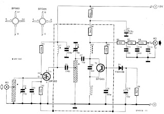
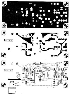
It is a super-regenerative type with an active RF amplifier, T1. The antenna signal is applied to the input inductor via a BNC socket, K1. The input circuit is tuned by trimmer C4. The amplified RF signal is applied to the input of the super-regenerative stage based on transistor T2. Although the oscillator is, strictly speaking, not tuned, it will lock on to the amplified RF signal applied via coupling capacitor C7. The low-frequency modulation component is extracted from the oscillator signal with the aid of low-pass filter, R6-R7-C12-R8-C13. The signal level at the demodulator output is 50 to 800 mVpp, so that further amplification is required·before the signal can be applied to a digital input. The inductors in the RF amplifier input and output are made from 1 mm dia. silver-plated wire. The length of the pieces of wire is indicated by the component overlay. The wires run at a height of about 3 mm above the board surface. Note that the stator terminal of C4 is bent upwards and soldered direct to the input inductor. The same goes for junction C6-C7, which is soldered ‘in the air‘, directly op to the hot end of the inductor wire. Inductor L1 consists of 12 turns of 0.6-mm dia. enamelled copper wire. Its internal diameter is 3 mm. Each of chokes g and L3 consists of 4 turns of 0.2-mm dia enamelled copper wire through a 3 mm long ferrite bead. Capacitor C8 is a surface-mount technology (SMT) type which is fitted at the solder side of the board, as are the BFG65 and the BFQSO. The type indica- tion printed on the transistors is legible from the component side of the board. As indicated by the dashed lines on the component overlay, the super-regenerative section of the circuit must be screened from the rest. To do this, it is best to solder a 20 mm high tin plate box on to the PCB as indicated.
Thursday, 22 December 2016
Lights Control for Model Cars Circuit Diagram
Lights Control for Model Cars Circuit Diagram
The basic idea was to tap into the signal from the radio control receiver and, with a bit of help from a microcontroller, simulate indicators using flashing yellow LEDs and brake lights using red LEDs. Further red LEDs are used for the tail lights, and white LEDs for the headlights. Connectors JP4 and JP5 (channel 0) are wired in parallel, as are JP6 and JP7 (channel 1), allowing the circuit to be inserted into the servo control cables for the steering and drive motor respectively. The ATtiny45 micro-controller takes power from the radio receiver via diode D1. T1 and T2 buffer the servo signals to protect IC1’s inputs from damage.
JP3 is provided to allow the use of a separate lighting supply. This can either be connected to an additional four-cell battery pack or to the main supply for the drive motor. The val-ues given for resistors R8 to R17 are suitable for use with a 4.8 V supply. JP2 can take the form of a 2x10 header.
As usual the sof t ware is available as a free download from the Elektor web pages accom-panying this article[1], and ready-programmed microcontrollers are also available. The microcontroller must be taught what servo signals correspond to left and right turns, and to full throttle and full braking. First connect the fin-ished circuit to the radio control electronics in the car, making sure everything is switched of f. Fit jumper JP1 to enable configuration mode, switch on the radio control transmit-ter, set all proportional controls to their cen-tre positions, and then switch on the receiver. The indicator LEDs should first flash on both sides. Then the car will indicate left for 3 s: during this time quickly turn the steering on the radio control transmitter fully to the left and the throt tle to full reverse (maximum braking).
Hold the controls in this position until the car starts to indicate right. Then set the controls to their opposite extremes and hold them there until both sides flash again. Now, if the car has an internal combustion engine (and so cannot go in reverse), keep the throttle control on full; if the car has an electric motor, set the throttle to full reverse. Hold this position while both sides are flashing. Configuration is now complete and JP1 can be removed. If you make a mistake during the configuration process, start again from the beginning.
Tuesday, 20 December 2016

Friday, 9 December 2016
0 30V Stabilized Variable Power Supply with Current Control

This is high quality stabilized power supply circuit diagram. You will able to adjust the output voltage from 0 volt up to 30 volt DC. You also able to adjust the current output value from 0.002 A to 3 A. This variable power supply incorporates an electronic output current limiter that effectively controls the output current from a few mA (2 mA) to the maximum output of 3 A that the circuit can produce.
Component list:
R1 = 2,2 KOhm 1W
R2 = 82 Ohm 1/4W
R3 = 220 Ohm 1/4W
R4 = 4,7 KOhm 1/4W
R5, R6, R13, R20, R21 = 10 KOhm 1/4W
R7 = 0,47 Ohm 5W
R8, R11 = 27 KOhm 1/4W
R9, R19 = 2,2 KOhm 1/4W
R10 = 270 KOhm 1/4W
R12, R18 = 56KOhm 1/4W
R14 = 1,5 KOhm 1/4W
R15, R16 = 1 KOhm 1/4W
R17 = 33 Ohm 1/4W
R22 = 3,9 KOhm 1/4W
RV1 = 100K trimmer
P1, P2 = 10KOhm linear pontesiometer
C1 = 3300 uF/50V electrolytic
C2, C3 = 47uF/50V electrolytic
C4 = 100nF polyester
C5 = 200nF polyester
C6 = 100pF ceramic
C7 = 10uF/50V electrolytic
C8 = 330pF ceramic
C9 = 100pF ceramic
D1, D2, D3, D4 = 1N5402,3,4 diode 2A – RAX GI837U
D5, D6 = 1N4148
D7, D8 = 5,6V Zener
D9, D10 = 1N4148
D11 = 1N4001 diode 1A
Q1 = BC548, NPN transistor or BC547
Q2 = 2N2219 NPN transistor
Q3 = BC557, PNP transistor or BC327
Q4 = 2N3055 NPN power transistor
U1, U2, U3 = TL081, operational amplifier
D12 = LED diode
Sunday, 4 December 2016
0 30V Stabilized Variable Power Supply with Current Control
This is high quality stabilized power supply circuit diagram. You will able to adjust the output voltage from 0 volt up to 30 volt DC. You also able to adjust the current output value from 0.002 A to 3 A. This variable power supply incorporates an electronic output current limiter that effectively controls the output current from a few mA (2 mA) to the maximum output of 3 A that the circuit can produce.
Component list:
R1 = 2,2 KOhm 1W
R2 = 82 Ohm 1/4W
R3 = 220 Ohm 1/4W
R4 = 4,7 KOhm 1/4W
R5, R6, R13, R20, R21 = 10 KOhm 1/4W
R7 = 0,47 Ohm 5W
R8, R11 = 27 KOhm 1/4W
R9, R19 = 2,2 KOhm 1/4W
R10 = 270 KOhm 1/4W
R12, R18 = 56KOhm 1/4W
R14 = 1,5 KOhm 1/4W
R15, R16 = 1 KOhm 1/4W
R17 = 33 Ohm 1/4W
R22 = 3,9 KOhm 1/4W
RV1 = 100K trimmer
P1, P2 = 10KOhm linear pontesiometer
C1 = 3300 uF/50V electrolytic
C2, C3 = 47uF/50V electrolytic
C4 = 100nF polyester
C5 = 200nF polyester
C6 = 100pF ceramic
C7 = 10uF/50V electrolytic
C8 = 330pF ceramic
C9 = 100pF ceramic
D1, D2, D3, D4 = 1N5402,3,4 diode 2A – RAX GI837U
D5, D6 = 1N4148
D7, D8 = 5,6V Zener
D9, D10 = 1N4148
D11 = 1N4001 diode 1A
Q1 = BC548, NPN transistor or BC547
Q2 = 2N2219 NPN transistor
Q3 = BC557, PNP transistor or BC327
Q4 = 2N3055 NPN power transistor
U1, U2, U3 = TL081, operational amplifier
D12 = LED diode
Tuesday, 29 November 2016
3 Band Tone Control Circuit
Figure Series 3 Band Tone Control

Tuesday, 22 November 2016
LBL Activated Remote Control Circuit Diagram
LBL Activated Remote Control Circuit Diagram

The circuit idea may be understood with the below mentioned points:
- Transistor T1 alnog with R3, C6 and the LDR itself forms a simple light sensor stage.
- The LDR is connected across the base of the transistor and the positive supply such that when light falls over the LDR, T1 receives the required base bias and conducts.
- When T1 conducts, the high potential at pin 14 of IC1 is pulled to logic low. However since a logic low wouldn't effect pin#14, IC1 does not respond as yet.
- The moment light on the LDR is switched OFF, T1 is switched OFF and pin#14 now instantly receives a subsequent logic high via R5.....now IC1 responds, and shifts it's output from pin#3 to pin#2. This makes pin#3 logic low, activating T2, and the preceding relay driver stage.
- The above condition persists until the LDR is illuminated again with a flashlight or with a laser beam.
- The above operation alternately toggles the output ON and OFF providing the required toggling actions to the connected load.
- The LDR must be covered inside an opaque pipe, about an inch long so that the ambient light stays obstructed from the LDR.
- The angle of the pipe should be kept in a such a way that it facilitates easy focusing of the light beam toward the LDR.
- C6 ensures that the system does not respond to accidental spurious light beams in case it finds its way inside the pipe, and over the LDR.
Parts List
- R3,R4,R5,R6,R7 = 2K2
- T1 = BC547,
- T2 = BC557
- IC1 = 4017
- IC2 = 7812
- ALL DIODES = 1N4007
- C6,C7 = 10uF/25V
- C8 = 1000uF/25V
- C10 = 0.1uF