Showing posts with label FM. Show all posts
Showing posts with label FM. Show all posts
Tuesday, 7 March 2017
FM Beacon Broadcast Transmitter 88 108 MHz Circuit
Frequency modulated broadcast band of 88 Mhz to 108 Mhz shall be used to transmit an audio tone. A distance of 100 yards is a working distance for such a broadcast band to be used by this circuit.
A popular timer 555 is being used to produce the tone that is nearly 600 Hz. The frequency modulates a heartly oscillator. The oscillator frequency is governed by an inductance and a capacitance.
The inductor is primarily an air core inductor which is built around a G.I. or M.S. bolt having 3*16 inches diameter. The bolt is basically a plain Hanger bolt termed as #8x32. Five turns are wound on the bolt and then the bolt is carefully removed by unscrewing.
After the coil is made it is stretched to 3* 8 inches and tapped at the centre. The frequency of the oscillation should be kept for best results at the centre of the band, i.e. 88 to 100 MHz. This can be shifted high or low by expanding or compressing the inductance coil. The 555 timer which produces the tone of around 600 Hz modulates the heartly oscillator. The output from the J-FET (2N4392) has the same phase as a signal at its gate and has the same voltage as input, where as the current is being amplified and thus acting as a current buffer.
A small signal diode (IN914/ IN4148) is being used here as a varactor Diode. This varactor diode is also termed as variable capacitor diode or variable reactance or variable cup diode whose capacitance varies as a function of the voltage across its anode and cathode and thus also being termed as a tuning diode. The total capacity in parallel with the inductor varies at the audio rate causing the oscillator frequency to change accordingly.
The ramping wave at Pin 2 and 6 of the timer circuit is being applied to the reverse bias diode through the IM resistance. This enables the capacitance of the diode to change as the ramping voltage changes. This alters the frequency of the tank circuit. An alternative methodology could have been employed so that an audio signal is fed to the IM resistance to modulate the oscillator but it would have required an additional pull up resistance to reverse bias the diodes.
The principle of the varactor diodes is very interesting as they operate in reverse bias condition. The thickness of the depletion Layer varies with the applied voltage and despite that there is no current through it. Its capacitance varies with the applied voltage. Actually the thickness of the depletion region varies to the square root of the applied voltage, as capacitance is inversely proportional to the depletion region thickness.
All components used in the circuit are readily available from radio shacks. The J-FET transistors must be of high frequency response.


Wednesday, 1 March 2017
TDA1599 IF amplifier demodulator for FM radio receivers
Circuit Diagram:
 |
| TDA1599 IF amplifier/demodulator for FM radio receivers |
Saturday, 4 February 2017
USB FM transmitter circuit

Here's a simple VHF FM transmitter that could be used to play audio files from an MP3 player or computer on a standard VHF FM radio. The circuit use no coils that have to be wound. This FM transmitter can be used to listen to your own music throughout your home. When this FM transmitter used in the car, there is no need for a separate input to the car stereo to play back the music files from your MP3 player.
To keep the circuit simple as well as compact, it was decided to use a chip made by Maxim Integrated Products, the MAX2606 [1]. This IC from the MAX2605-MAX2609 series has been specifically designed for low-noise RF applications with a fixed frequency. The VCO (Voltage Controlled Oscillator) in this IC uses a Colpitts oscillator circuit. The variable-capacitance (varicap) diode and feedback capacitors for the tuning have also been integrated on this chip, so that you only need an external inductor to fix the central oscillator frequency.
 |
| USB FM transmitter schematics |
It is possible to fine-tune the frequency by varying the voltage to the varicap. Not much is demanded of the inductor, a type with a relatively low Q factor (35 to 40) is sufficient according to Maxim. The supply voltage to the IC should be between 2.7 and 5.5 V, the current consumption is between 2 and 4 mA. With values like these it seemed a good idea to supply the circuit with power from a USB port.
A common-mode choke is connected in series with the USB connections in order to avoid interference between the circuit and the PC supply. There is not much else to the circuit. The stereo signal connected to K1 is combined via R1 and R2 and is then passed via volume control P1 to the Tune input of IC1, where it causes the carrier wave to be frequency modulated. Filter R6/C7 is used to restrict the bandwidth of the audio signal. The setting of the frequency (across the whole VHF FM broadcast band) is done with P2, which is connected to the 5 V supply voltage.
The PCB designed uses resistors and capacitors with 0805 SMD packaging. The size of the board is only 41.2 x 17.9 mm, which is practically dongle-sized. For the aerial an almost straight copper track has been placed at the edge of the board. In practice we achieved a range of about 6 metres (18 feet) with this. There is also room for a 5-way SIL header on the board. Here we find the inputs to the 3.5 mm jack plug, the input to P1 and the supply voltage. The latter permits the circuit to be powered independently from the mains supply, via for example three AA batteries or a Lithium button cell. Inductor L1 in the prototype is a type made by Murata that has a fairly high Q factor: minimum 60 at 100 MHz.
 |
| Layout PCB USB FM transmitter |
Take care when you solder filter choke L2, since the connections on both sides are very close together. The supply voltage is connected to this, so make sure that you don’t short out the USB supply! Use a resistance meter to check that there is no short between the two supply connectors before connecting the circuit to a USB port on a computer or to the batteries.
P1 has the opposite effect to what you would expect (clockwise reduces the volume), because this made the board layout much easier. The deviation and audio bandwidth varies with the setting of P1. The maximum sensitivity of the audio input is fairly large. With P1 set to its maximum level, a stereo input of 10 mVrms is sufficient for the sound on the radio to remain clear. This also depends on the setting of the VCO. With a higher tuning voltage the input signal may be almost twice as large (see VCO tuning curve in the data sheet). Above that level some audible distortion becomes apparent. If the attenuation can’t be easily set by P1, you can increase the values of R1 and R2 without any problems.
Measurements with an RF analyzer showed that the third harmonic had a strong presence in the transmitted spectrum (about 10 dB below the fundamental frequency). This should really have been much lower. With a low-impedance source connected to both inputs the bandwidth varies from 13.1 kHz (P1 at maximum) to 57 kHz (with the wiper of P1 set to 1/10).
In this circuit the pre-emphasis of the input is missing. Radios in Europe have a built-in de-emphasis network of 50 μs (75 μs in the US). The sound from the radio will therefore sound noticeably muffled. To correct this, and also to stop a stereo receiver from mistakenly reacting to a 19 kHz component in the audio signal, an enhancement circuit Is published elsewhere in this issue (Pre-emphasis for FM Transmitter, also with a PCB). Author: Mathieu Coustans, Elektor Magazine, 2009
MP3 FM Transmitter Parts List
Resistors (all SMD 0805)
R1,R2 = 22kΩ
R3 = 4kΩ7
R4,R5 = 1kΩ
R6 = 270Ω
P1 = 10kΩ preset, SMD (TS53YJ103MR10 Vishay Sfernice, Farnell # 1557933)
P2 = 100kΩ preset, SMD(TS53YJ104MR10 Vishay Sfernice, Farnell # 1557934)
Capacitors (all SMD 0805)
C1,C2,C5 = 4μF7 10V
C3,C8 = 100nF
C4,C7 = 2nF2
C6 = 470nF
Inductors
L1 = 390nF, SMD 1206 (LQH31HNR39K03L Murata, Farnell # 1515418)
L2 = 2200Ω @ 100MHz, SMD, common-mode choke, 1206 type(DLW31SN222SQ2L Murata, Farnell #1515599)
Semiconductors
IC1 = MAX2606EUT+, SMD SOT23-6 (Maxim Integrated Products)
Miscellaneous
K1 = 3.5mm stereo audio jack SMD (SJ1-3513-SMT
CUI Inc, DIGI-Key # CP1-3513SJCT-ND)
K2 = 5-pin header (only required in combination with 090305-I pre-emphasis circuit)
K3 = USB connector type A, SMD (2410 07 Lumberg, Farnell # 1308875)
Notice. The use of a VHF FM transmitter, even a low power device like the one described here, is subject to radio regulations and may not be legal in all countries.
source [ Link ]
source [ Link ]
Thursday, 2 February 2017
Single chip FM transmitter circuit
Description
Here’s a single chip FM transmitter circuit using Maxim semiconductors IC MAX2606. The MAX2606 is a compact, high-performance intermediate frequency VCO specially designed for wireless communication circuits. They have monolithic construction with low-noise and a low-power operation in a compact 6-pin SOT23 packing .Th1s low-noise IC feature an on-chip varicap diode and feedback capacitances that avoid the need for external tuning components, making the MAX2606 perfect for portable systems. Only an external inductor is needed to set the oscillation frequency.In addition to this, an
integrated differential output buffer is also there for driving a mixer or prescaler.The MAX2606 can be operated from a single +2.8 V to +5.4V supply and consumes very less current .The chip can be operated from 45MHz to 650MHz .
integrated differential output buffer is also there for driving a mixer or prescaler.The MAX2606 can be operated from a single +2.8 V to +5.4V supply and consumes very less current .The chip can be operated from 45MHz to 650MHz .
In the circuit the nominal frequency is set to 100 Mhz by inductor L1, (390nH) . The left and right channel audio signals from your source are added by R3 and R4, and attenuated by the POT R2. R2 can be used as a volume control .POT R1 can be used to select a channel of transmission between 88Mhz and 108Mhz.Use 80 cm long wire as the antenna .
FM Transmitter Circuit Diagram with Parts List.

Single Chip FM Transmitter Circuit Diagram
Notes
- Assemble the circuit on a good quality PCB or common board.
- Use a battery for powering the circuit.It will reduce noise.
- An FM antenna from a old radio is a better option than the wire antenna.
Saturday, 14 January 2017
1 watt 10km FM Transmitter Circuit
In this article we learn about a 1 Watt FM Transmitter amplifier with a reasonably balanced design specified to boost a RF frequency in the 88 – 108 MHz spectrum.
It may be considered a fairly sensitive configuration when used with quality RF power amplifier transistors, trimmers and inductors. It involves a power amplification factor of 9 to 12 dB (9 to 15 times). At an input power of 0.1W the output may be well over 1W. It's advisable to choose T1 transistor on the basis of the fed voltage. Considering you possess a 12V power supply in that case using transistors like: 2N4427, KT920A, KT934A, KT904, BLX65, 2SC1970, BLY87. At 18 to 24V inputs you may want to use transistors such as: 2N3866, 2N3553, KT922A, BLY91, BLX92A. You could also consider using 2N2219 at 12V However that would yield just an output power of 0.4W at the fullest.

How to Calibrate this 1 watt fm power amp
Initially don't apply any sort of RF input, simply use the power and check with a meter the voltage at point 1. Calibrate R3 as you get the reading near about 0.7V. Use the antenna with a 2 x 100 Ω 0.5W resistors in parallel at the RF output. After this attach the rf source that may be supposed to boost and link up this RF input to the output.
Carefully set up C1 so as to extract the most optimal potential magnitude on the rf link. Next up, rotate R3 once more to acquire 0.7 V at point 1. Finally set up C5 and C6 for ensuring the highest output voltage (quite between 12V to 18V).
Verify the dissipation of T1′s heatsink, if you see it to be just fine switch off the power, isolate and pull of the 2 resistors of 100 Ω and connect back the antenna (make sure the the probe stays connected). Connect again the power and yet again allign C1, C5 and C6 for highest voltage read on the probe.
You could think of using a an ammeter for enabling reading the current incourse via T1. This must be restricted below 150mA at 12V and 100mA at 24V otherwise the transistor may well fry of. L2 and L3 coils must be installed at an angle of 90 degrees between the two. Don’t run the 1W rf fm amplifier in case you witness your TV set is getting jammed and perhaps the laws of the your country prohibits the use of such FM transmitters.BOM for the above 10km FM transmitter
R1 = 100 Ω
R2 = 2.2K Ω for 12 V and 4.7 kΩ for 24 V
R3 = 10 KΩ
R4 = 100 Ω
C1 = C5 = C6 = 10 – 60 pF
C2 = C4 = 1 nF
C3 = 10 uF
D1 = 1N4148
L1 = 20 turns of 0.2mm super enameled wire over R4
L2 = 7 turns of 0.8mm super enameled wire with 6mm diameter on air
L3 = 4 turns of 0.8mm super enameled wire with 7mm diameter on air
T1 = 2N4427, KT920A, KT934A, KT904, BLX65, 2SC1970, BLY87 (2N2219, output of 0.4W) at 12V
T1 = 2N3866, 2N3553, KT922A, BLY91, BLX92A at 24V
It may be considered a fairly sensitive configuration when used with quality RF power amplifier transistors, trimmers and inductors. It involves a power amplification factor of 9 to 12 dB (9 to 15 times). At an input power of 0.1W the output may be well over 1W. It's advisable to choose T1 transistor on the basis of the fed voltage. Considering you possess a 12V power supply in that case using transistors like: 2N4427, KT920A, KT934A, KT904, BLX65, 2SC1970, BLY87. At 18 to 24V inputs you may want to use transistors such as: 2N3866, 2N3553, KT922A, BLY91, BLX92A. You could also consider using 2N2219 at 12V However that would yield just an output power of 0.4W at the fullest.
How to Calibrate this 1 watt fm power amp
Initially don't apply any sort of RF input, simply use the power and check with a meter the voltage at point 1. Calibrate R3 as you get the reading near about 0.7V. Use the antenna with a 2 x 100 Ω 0.5W resistors in parallel at the RF output. After this attach the rf source that may be supposed to boost and link up this RF input to the output.
Carefully set up C1 so as to extract the most optimal potential magnitude on the rf link. Next up, rotate R3 once more to acquire 0.7 V at point 1. Finally set up C5 and C6 for ensuring the highest output voltage (quite between 12V to 18V).
Verify the dissipation of T1′s heatsink, if you see it to be just fine switch off the power, isolate and pull of the 2 resistors of 100 Ω and connect back the antenna (make sure the the probe stays connected). Connect again the power and yet again allign C1, C5 and C6 for highest voltage read on the probe.
You could think of using a an ammeter for enabling reading the current incourse via T1. This must be restricted below 150mA at 12V and 100mA at 24V otherwise the transistor may well fry of. L2 and L3 coils must be installed at an angle of 90 degrees between the two. Don’t run the 1W rf fm amplifier in case you witness your TV set is getting jammed and perhaps the laws of the your country prohibits the use of such FM transmitters.
R1 = 100 Ω
R2 = 2.2K Ω for 12 V and 4.7 kΩ for 24 V
R3 = 10 KΩ
R4 = 100 Ω
C1 = C5 = C6 = 10 – 60 pF
C2 = C4 = 1 nF
C3 = 10 uF
D1 = 1N4148
L1 = 20 turns of 0.2mm super enameled wire over R4
L2 = 7 turns of 0.8mm super enameled wire with 6mm diameter on air
L3 = 4 turns of 0.8mm super enameled wire with 7mm diameter on air
T1 = 2N4427, KT920A, KT934A, KT904, BLX65, 2SC1970, BLY87 (2N2219, output of 0.4W) at 12V
T1 = 2N3866, 2N3553, KT922A, BLY91, BLX92A at 24V
Sony ST S333ESG FM stereo FM AM tuner circuit diagram


Thursday, 12 January 2017
Transmitter FM 45W with valve
TECHNICAL CHARACTERISTICS:
 Materially:
Most elements you can him find in a old back-white television with lamps.
Regulations:
Notes:
Source http://www.electronics-lab.com/
- Tendency of catering: 220V AC
- Frequency of emission at FM: 88~108MHz
- Force of expense: max 45W (without the R3)
- R1 15KW/2W
- R2 1KW/10W
- R3 1KW/10W (for biggest force in the exit you replace with short-circuit).
- C1 50pF trimmer
- C2 30pF trimmer
- C3 22pF/4KV
- C4, c6, c9 10nF/1KV
- C5, c7 1nF/1KV
- C8 100mF+100mF/450V (Double electrolytic)
- C9, c10 10nF
- RFC1, rfc2, rfc3 air Inductors: 15 coils diameter 8mm, from wire 1mm.
- T1 Transformer 220V/6V-1A
- T2 Transformer of configuration with being first 4 or 8W
- T3 Inductor with core ferrite (externally it resembles with small transformer but has a turn only).
- D1 BY127 rectifier
- Lamp 807 SYLV USA or EL34 or equivalent
- ANTENNA Simple dipole L/2. (L= wave length)
- S1 Main switch of catering.
- S2 Switch of catering of rise (him we close after zestacej' the thread).
Regulations:
- With the C2 we regulate the frequency.
- With the C1 we adapt the resistance of aerial (practically him we regulate so that it is heard our voice in the radio as long as you become cleaner).
- The catering better it does not become at straight line from the network 220V but via transformer 220V/220V of isolation and safety 1A.
- When does not exist the R3, the force of expense is bigger, but respectively is increased also the hum 50Hz, because the simplicity of designing.
- The control (Audio In) can become from a kasseto'fwno or other powerful source. If it is microphone it will be supposed precedes amplifier so that it acquires a force of order of 8W roughly.
Source http://www.electronics-lab.com/
Stereo FM transmitter circuit using BA1404
Notes.
A high quality stereo FM transmitter circuit is shown here. The circuit is based on the IC BA1404 from ROHM Semiconductors. BA1404 is a monolithic FM stereo modulator that has built in stereo modulator, FM modulator, RF amplifier circuitries. The FM modulator can be operated from 76 to 108MHz and power supply for the circuit can be anything between 1.25 to 3 volts.
In the circuit R7, C16, C14 and R6, C15, C13 forms the pre-emphasis network for the right and left channels respectively. This is done for matching the frequency response of the FM transmitter with the FM receiver. Inductor L1 and capacitor C5 is used to set the oscillator frequency. Network C9,C10, R4,R5 improves the channel separation. 38kHz crystal X1 is connected between pins 5 and 6 of the IC. Composite stereo signal is created by the stereo modulator circuit using the 38kHz quartz controlled frequency.
Circuit diagram.
A high quality stereo FM transmitter circuit is shown here. The circuit is based on the IC BA1404 from ROHM Semiconductors. BA1404 is a monolithic FM stereo modulator that has built in stereo modulator, FM modulator, RF amplifier circuitries. The FM modulator can be operated from 76 to 108MHz and power supply for the circuit can be anything between 1.25 to 3 volts.
In the circuit R7, C16, C14 and R6, C15, C13 forms the pre-emphasis network for the right and left channels respectively. This is done for matching the frequency response of the FM transmitter with the FM receiver. Inductor L1 and capacitor C5 is used to set the oscillator frequency. Network C9,C10, R4,R5 improves the channel separation. 38kHz crystal X1 is connected between pins 5 and 6 of the IC. Composite stereo signal is created by the stereo modulator circuit using the 38kHz quartz controlled frequency.
Circuit diagram.

Stereo FM transmitter circuit
- Assemble the circuit on a good quality PCB.
- Powering the circuit from a battery will reduce noise.
- Use an 80 cm copper wire as antenna.
- For L1 make 3 turns of 0.5mm dia enamelled copper wire on a 5mm dia ferrite core.
Saturday, 31 December 2016
UHF FM Remote Control Receiver Circuit
The receiver is intended primarily for use with the remote control UHF transmitter described in the preceding article.
It is a super-regenerative type with an active RF amplifier, T1. The antenna signal is applied to the input inductor via a BNC socket, K1. The input circuit is tuned by trimmer C4. The amplified RF signal is applied to the input of the super-regenerative stage based on transistor T2. Although the oscillator is, strictly speaking, not tuned, it will lock on to the amplified RF signal applied via coupling capacitor C7. The low-frequency modulation component is extracted from the oscillator signal with the aid of low-pass filter, R6-R7-C12-R8-C13. The signal level at the demodulator output is 50 to 800 mVpp, so that further amplification is required·before the signal can be applied to a digital input. The inductors in the RF amplifier input and output are made from 1 mm dia. silver-plated wire. The length of the pieces of wire is indicated by the component overlay. The wires run at a height of about 3 mm above the board surface. Note that the stator terminal of C4 is bent upwards and soldered direct to the input inductor. The same goes for junction C6-C7, which is soldered ‘in the air‘, directly op to the hot end of the inductor wire. Inductor L1 consists of 12 turns of 0.6-mm dia. enamelled copper wire. Its internal diameter is 3 mm. Each of chokes g and L3 consists of 4 turns of 0.2-mm dia enamelled copper wire through a 3 mm long ferrite bead. Capacitor C8 is a surface-mount technology (SMT) type which is fitted at the solder side of the board, as are the BFG65 and the BFQSO. The type indica- tion printed on the transistors is legible from the component side of the board. As indicated by the dashed lines on the component overlay, the super-regenerative section of the circuit must be screened from the rest. To do this, it is best to solder a 20 mm high tin plate box on to the PCB as indicated.
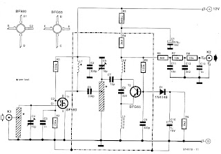
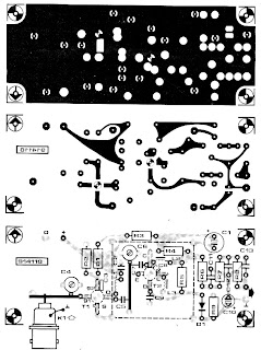
It is a super-regenerative type with an active RF amplifier, T1. The antenna signal is applied to the input inductor via a BNC socket, K1. The input circuit is tuned by trimmer C4. The amplified RF signal is applied to the input of the super-regenerative stage based on transistor T2. Although the oscillator is, strictly speaking, not tuned, it will lock on to the amplified RF signal applied via coupling capacitor C7. The low-frequency modulation component is extracted from the oscillator signal with the aid of low-pass filter, R6-R7-C12-R8-C13. The signal level at the demodulator output is 50 to 800 mVpp, so that further amplification is required·before the signal can be applied to a digital input. The inductors in the RF amplifier input and output are made from 1 mm dia. silver-plated wire. The length of the pieces of wire is indicated by the component overlay. The wires run at a height of about 3 mm above the board surface. Note that the stator terminal of C4 is bent upwards and soldered direct to the input inductor. The same goes for junction C6-C7, which is soldered ‘in the air‘, directly op to the hot end of the inductor wire. Inductor L1 consists of 12 turns of 0.6-mm dia. enamelled copper wire. Its internal diameter is 3 mm. Each of chokes g and L3 consists of 4 turns of 0.2-mm dia enamelled copper wire through a 3 mm long ferrite bead. Capacitor C8 is a surface-mount technology (SMT) type which is fitted at the solder side of the board, as are the BFG65 and the BFQSO. The type indica- tion printed on the transistors is legible from the component side of the board. As indicated by the dashed lines on the component overlay, the super-regenerative section of the circuit must be screened from the rest. To do this, it is best to solder a 20 mm high tin plate box on to the PCB as indicated.
For the transmitter circuit : UHF FM Remote Control Transmitter Circuit
Friday, 23 December 2016
DIY Micromitter Stereo FM Transmitter
This new stereo FM Micromitter is capable of broadcasting good quality signals over a range of about 20 metres. It`s ideal for broadcasting music from a CD player or from any other source so that it can be picked up in another location. For example, if you don`t have a CD player in you car, you can use the Micromitter to broadcast signals from a p visit page.
 |
| DIY Micromitter Stereo FM Transmitter |
Sunday, 18 December 2016
4W FM Transmitter Circuit
TECHNICAL CHARACTERISTICS:
Circuit Diagram:
 Materially:
PCB:
Before you print it out with microsoft paints, set the screen resolution to 1280 by 1024 in order to get the correct scale
 Regulations:
Notes:
The T2 wants refrigerator.
Author: Kyriakos Kontakos, kkontak@hotmail.com
Source http://www.electronics-lab.com/
- Stabilised tendency of catering: Vcc=12~16V
- Frequency of emission: 88~108MHz
- Consumption: 100~400mA
- The resistors are 1/4W.
- R1, R2 10KOhm
- R3 47Ohm
- C1, C2 1nF
- C3 4,7uF/16V
- C4, C7, C8 0~45pF trimmer
- C5, C6 10pF
- C9 100nF
- L1 4 turns, 7mm diameter *
- L3 3 turns, 7mm diameter *
- L4 5 turns, 7mm diameter *
- L2 RFC (resistance 1MOhm with wrapped around her inductor of enough coils from fine isolated wire. Scratch of utmost inductor and you stick in utmost the resistance making thus a parallel L-r circuit.)
- T1, T2 2N2219
- ANT Simple dipole l/2.
- MIC IN Microphone dynamic or other type. (It can also connected to a cassette player unit)
- * The inductors is air from wire of coaxial 75W or other 1mm roughly.
Before you print it out with microsoft paints, set the screen resolution to 1280 by 1024 in order to get the correct scale
- With the C4 we regulate the frequency.
- With their C7, C8 we adapt the resistance of aerial (practically to them we regulate so that it is heard our voice in the radio as long as you become cleaner).
The T2 wants refrigerator.
Author: Kyriakos Kontakos, kkontak@hotmail.com
Source http://www.electronics-lab.com/
Saturday, 19 November 2016
Wave antenna 5 8 pro VKV FM
Wave antenna 5/8 consists of a vertical radiator which is fed at the base of the antenna. A suitable device of some sort should be added between the antenna and feedline if you want to eat with coax. Adding a coil in series with the antenna on the base is one of these methods are suitable.


So why would anyone use an antenna 5/8 wave if they have to go through all that extra work? After all, a ground plane antenna provides a good match. There are several answers. The first is GAIN. The computer shows that the antenna (mounted 1 foot above the ground) has a margin of about 1.5 dBd higher than a dipole (also installed 1 foot above the ground.)The second reason you might want to use the wave 5/8 vertical is to get a lower angle of radiation. Peak radiation angle A half-wave antenna is 20 degrees. You will find that the angle 5/8 wave antenna radiation is only 16 degrees so it is better dx antenna.
You may have noticed a pattern developing here. A quarter-wave ground plane antenna has a radiation pattern that produces the maximum gain at about 25 degrees and half-wave antenna drops to 20-degree angle, and wave antenna 5/8 further drops to 16 degrees angle. So why not just keep extending the antenna to one full wave? Well it would be nice if it worked, but unfortunately the wave patterns begin to create a very high angle of radiation waves exceed 5/8. So we've reached the maximum gain at this point and extend the antenna further reduce profits only where we want it (low angle).
Of course if you are interested in a very short jump, extend the antenna will produce a nice profit on the dipole.All the length of the antenna depends on various factors. Some of these factors are: height above ground, the diameter of the wire, nearby structures, the effects of other antennas in the area and even the conductivity of the soil.This page allows you to calculate the wavelength for the antenna 5/8. It uses the standard formula, 585 / f (178.308 / f for metric) MHz to calculate the length of the element. If you have experimented with 5/8 wave antenna before and know a better formula for your QTH, feel free to change the formula accordingly. This formula is for the antenna wire.
Of course if you build your antenna out of the tube, total length of the antenna will be shorter, for example I have found that 21.5 feet seems to provide maximum benefit to the frequency of 28.5 MHz when using a 1 "tube, and 22.5. Foot seems be the best long-wire at the same frequency. Since the formula to calculate the antenna to be about 2 feet shorter, be sure to experiment and maybe add a little for your final term.
Wednesday, 16 November 2016
Low Cost 3 volts FM Transmitter
This very Simple Electronic Project and useful circuit diagram of an FM transmitter is sown in this schematic. This fm transmitter circuit is very simple and it has a acceptable transmission. The signal transited from this fm transmitter circuit can be received at almost 300 meters in open air The circuit require a 3volts operating voltage and can be tuned anywhere in the FM band.
Low-Cost 3 volts FM Transmitter Circuit Diagram:

You can use this rf transmitter circuit to transmit signal from your house to garden or from room to room . To listen the signal you can use any radio (portable or not ) that can work on FM band . The coil should be about 3mm in diameter and 5 turns. The wire is tinned copper wire, 0.61 mm in diameter.
After the coil in soldered into place spread the coils apart about 0.5 to 1mm so that they are not touching. If you don’t have a trim cap you can use a fixed value capacitor and you can vary the TX frequency by adjusting the spacing of the coils or placing a small piece of ferrite inside the coil, but the better way to change the transmission frequency is to use a variable capacitor.
Connect a half or quarter wavelength antenna (length of wire) to the aerial point. At an FM frequency of 100 MHz these lengths are 150 cm and 75 cm respectively. The calibration of this rf transmitter circuit is very simple and you need just to place a radio at some distance from the transmitter and set it somewhere about 89-90MHZ (chose the transmission frequency) and after that vary the transmitter oscillator frequency, by modifying the value of the capacitor. The transmission frequency is set to the desired frequency just when you can hear the transmitted signal.
Low-Cost 3 volts FM Transmitter Circuit Diagram:
You can use this rf transmitter circuit to transmit signal from your house to garden or from room to room . To listen the signal you can use any radio (portable or not ) that can work on FM band . The coil should be about 3mm in diameter and 5 turns. The wire is tinned copper wire, 0.61 mm in diameter.
After the coil in soldered into place spread the coils apart about 0.5 to 1mm so that they are not touching. If you don’t have a trim cap you can use a fixed value capacitor and you can vary the TX frequency by adjusting the spacing of the coils or placing a small piece of ferrite inside the coil, but the better way to change the transmission frequency is to use a variable capacitor.
Connect a half or quarter wavelength antenna (length of wire) to the aerial point. At an FM frequency of 100 MHz these lengths are 150 cm and 75 cm respectively. The calibration of this rf transmitter circuit is very simple and you need just to place a radio at some distance from the transmitter and set it somewhere about 89-90MHZ (chose the transmission frequency) and after that vary the transmitter oscillator frequency, by modifying the value of the capacitor. The transmission frequency is set to the desired frequency just when you can hear the transmitted signal.
Thursday, 3 November 2016
UHF FM Remote Control Transmitter Circuit
This low-power UHF FM transmitter is intended for remote control applications such as garage doors and wireless alarm systems.
It is a single transistor design that operates at a frequency reserved for low-power wireless signalling. The operating frequency is determined by a resonator, F11. The following types may be used: UK: Type R2528 for 418 MHz; USA: Type Rl53O for 315 MHz; Holland, Belgium, Germany: Type R2554 for 433;92 MHZ: France: Type R2523 for 224.5 MHZ. The transmitter is frequency-modulated by an audio (or digital) signal applied to the junction of a varactors D1, D2 via R3. The varactors effectively change the shunt capacitance of the resonator as a function of the modulation signal, which results in FM. The design may be changed to produce AM (amplitude-modulation) by omitting components D1, D2, R2, R3 and R6, and interconnecting points ‘A’ and ‘B‘. Transistor T1 is fitted at the solder side of the printed circuit board, as indicated by the dashed outline on the component overlay. Also on this side of the PCB is a short wire link (use silver plated wire) that connects strip line inductor L1 to the positive supply track that runs in parallel with it. The position of the wire link d·epends on the transmit frequency. The lower the frequency, the more inductance is required, that is, the further the link has to be ‘moved' towards the edge of the PCB. Some experimenting may be necessary to find the best position. Start by setting the trimmer, C3, about mid-way, and fit the wire link about ‘half way’ on the strip line. Monitor the received signal, and adjust C3 until a maximum is found. If you can not find,a maximum, try moving the wire link either towards the transistor (smaller inductance), or towards the PCB edge (greater inductance). The best position is that at which C3 ‘peaks‘ when set about mid-way. Since we are dealing with a UHF circuit, it goes without saying that all component terminals must be kept as short as possible. The transmitter must be housed in a plastic enclosure to enable it to radiate.


It is a single transistor design that operates at a frequency reserved for low-power wireless signalling. The operating frequency is determined by a resonator, F11. The following types may be used: UK: Type R2528 for 418 MHz; USA: Type Rl53O for 315 MHz; Holland, Belgium, Germany: Type R2554 for 433;92 MHZ: France: Type R2523 for 224.5 MHZ. The transmitter is frequency-modulated by an audio (or digital) signal applied to the junction of a varactors D1, D2 via R3. The varactors effectively change the shunt capacitance of the resonator as a function of the modulation signal, which results in FM. The design may be changed to produce AM (amplitude-modulation) by omitting components D1, D2, R2, R3 and R6, and interconnecting points ‘A’ and ‘B‘. Transistor T1 is fitted at the solder side of the printed circuit board, as indicated by the dashed outline on the component overlay. Also on this side of the PCB is a short wire link (use silver plated wire) that connects strip line inductor L1 to the positive supply track that runs in parallel with it. The position of the wire link d·epends on the transmit frequency. The lower the frequency, the more inductance is required, that is, the further the link has to be ‘moved' towards the edge of the PCB. Some experimenting may be necessary to find the best position. Start by setting the trimmer, C3, about mid-way, and fit the wire link about ‘half way’ on the strip line. Monitor the received signal, and adjust C3 until a maximum is found. If you can not find,a maximum, try moving the wire link either towards the transistor (smaller inductance), or towards the PCB edge (greater inductance). The best position is that at which C3 ‘peaks‘ when set about mid-way. Since we are dealing with a UHF circuit, it goes without saying that all component terminals must be kept as short as possible. The transmitter must be housed in a plastic enclosure to enable it to radiate.
The NEXT post discusses the Receiver Circuit: UHF FM Remote Control Receiver Circuit
Subscribe to:
Posts (Atom)