Showing posts with label Regulated. Show all posts
Showing posts with label Regulated. Show all posts
Tuesday, 10 January 2017
High Voltage Regulated with Foldback Current Limiting Circuit Diagram
This is a High Voltage Regulated with Foldback Current Limiting Circuit Diagram. The Foldback is a current limiting feature (a type of overload protection) of power supplies and power amplifiers. When the load attempts to draw over current from the supply, foldback reduces both the output voltage and current to well below the normal operating limits.
High Voltage with Foldback Current Limiting Circuit Diagram

Under a short circuit, where the output voltage has reduced to zero, the current is typically limited to a small fraction of the maximum current.This circuit use a TMOS MTM7N45 (Q2) is used as a series pass element in a linear high voltage supply that accepts +275-V unregulated and produces 250 V regulated with foldback current limiting.
A 15-V zener, Dlf provides the dc reference for operational amplifier Ul, whose other input is obtained from a fraction of the output voltage. Ul drives Q3, which drives the gate of Q2. Foldback current limiting is achieved by Rl, R2, R3, R4, Ql, and D2.

Wednesday, 28 December 2016
Pre regulated High Voltage Power Supply
This Pre-regulated High Voltage Power Supply Circuit Diagram triacs selects the tap on main transformer Tl, which provides the proper, pre-regulated voltage to the secondary regulator. T2 and its associated components comprise the secondary regulator. The ADC 0804, IC1, digitizes a voltage-feedback signal from the secondary regulator`s output.
Pre-regulated High Voltage Power Supply Circuit Diagram:
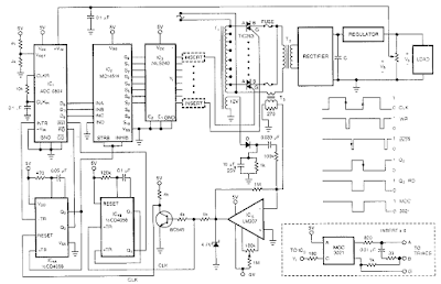
The MC1415 De-multiplexer, IC2, decodes the digitizer`s output. IC2, in turn, drives Tl`s opto-isolated triacs via the 74LS240 driver chip, IC3, and associated opto-isolators. Transformer T3 samples the circuit`s current output. The auxiliary, 12 V winding on Tl ensures noload starting. The combination of op amp IC5 and the inverting transistor, Ql, square this current signal.
The output of Ql is the CLK signal, which triggers one-half of the one shot, IC4A, to begin the circuit`s AID conversion. The one shots` periods are set to time out within 1l2 cycle of the ac input. Upon completion of its AID conversion, ICl`s INTR output triggers the other half of the one shot, IC4B, which enables the converter`s data outputs. The rising edge of the CLK signal resets the one shot and latches the new conversion value into IC2. The latch, associated driver, and optoisolator trigger a selected triac according to the latest value of the voltage-feedback signal, V, . Keep enjoying don't forget click on share button .
Pre-regulated High Voltage Power Supply Circuit Diagram:
The MC1415 De-multiplexer, IC2, decodes the digitizer`s output. IC2, in turn, drives Tl`s opto-isolated triacs via the 74LS240 driver chip, IC3, and associated opto-isolators. Transformer T3 samples the circuit`s current output. The auxiliary, 12 V winding on Tl ensures noload starting. The combination of op amp IC5 and the inverting transistor, Ql, square this current signal.
The output of Ql is the CLK signal, which triggers one-half of the one shot, IC4A, to begin the circuit`s AID conversion. The one shots` periods are set to time out within 1l2 cycle of the ac input. Upon completion of its AID conversion, ICl`s INTR output triggers the other half of the one shot, IC4B, which enables the converter`s data outputs. The rising edge of the CLK signal resets the one shot and latches the new conversion value into IC2. The latch, associated driver, and optoisolator trigger a selected triac according to the latest value of the voltage-feedback signal, V, . Keep enjoying don't forget click on share button .
Subscribe to:
Posts (Atom)