Tuesday 31 January 2017

Safety Guard Circuit Diagram


Protect your home appliances from voltage spikes with this simple time delay circuit. Whenever power to the appliances is switched on or resumes after mains failure, the oscillator starts oscillating and D5 blinks. This continues for three minutes. After that, Q14 output of IC CD4060 goes high to trigger the gate of the SCR through D4. At this moment, the voltage is available at the cathode of the SCR, which energizes the relay coil to activate the appliance and D6 glows. Switch SW1 is used for quick start without waiting for delay.

Circuit Diagram:

Safety Guard Circuit Diagram

 Parts:

R1 = 1M
R2 = 470R
R3 = 820R
R4 = 56K
R5 = 470R
R6 = 1K
R7 = 10K
C1 = 1kuF-25V
C2 = 100nF-63V
C3 = 0.02uF-63V
C4 = 10uF-25V
C5 = 10uF-25V
D1 = 1N4007
D2 = 1N4007
D3 = 1N4007
D4 = 1N4148
D5 = Red LEDs
D6 = Red LEDs
RL1 = 12V Relay
IC1 = AN7809
IC2 = CD4060
SW1 = Switch
T1 = 24V-AC Centre Tapped Transformer

Circuit Operation:

At the heart of the circuit is IC CD4060, which consists of two inverter gates for clock generation and a 14-bit binary ripple counter. Here the clock oscillations are governed by resistor R1 and capacitor C1. In this circuit, only two outputs of the IC (Q5 and Q14) have been used. Q5 is connected to an LED (D5) and Q14 is used to trigger the gate of the SCR through D4 as well as reset the counter. The anode of the SCR is connected to +9V and the cathode is connected to the relay coil. The other pin of the relay coil is connected to the negative supply, while its contacts are used for switching on the appliances.

Readmore → Safety Guard Circuit Diagram

SAMSUNG protect circuit with LA76931


Following is the protect circuit Samsung TV which use IC LA76931 as basic working the protect circuit. This Protect Circuit LA76891 located at pin-30 whichconnected to the collector of transistor Q902.In normal conditions the voltage at the base of Q902 is "low" and the voltage at pin-30 is "high". For the temporary crippling protect, it can be removed Q902 (or to the emitter-base short).

SAMSUNG protect circuit with LA76931
Sampling circuit protect from:

Vertical Protect. Pulses of the vertical-out rectified by diode D355, so that the base voltage is approximately 0.6V Q904 ,and collector voltage is 0v.
X-ray Protect (option). Sampled using a heater voltage of the circuit as shown below. Normal vltage in x-ray path to the base of Q902 is zero.
Samsung TV Protect Circuit

ABL protect. If there is damage to flyback voltage which can cause a high rise ABL, then protect circuit will actively work.
Readmore → SAMSUNG protect circuit with LA76931

Vice Control Music Outlet with SL517A


This is Vice Control Music Outlet circuit using SL517A, this electronic circuit project build a very easy. The circuit is shown in Figure, and it is composed of acoustic sensor, voice control IC, relay control circuit, song voice circuit and AC buck rectifier circuit.

Vice Control Music Outlet Circuit using SL517A:

Vice-Control
Vice-Control-Music

Voice control IC uses SL517A which contains high-gain amplifier, bistable flip-flop and buffer output level, and it has two packages of dual in-line and black ointment. Its internal functional block diagram is shown as below.

Readmore → Vice Control Music Outlet with SL517A

Power Supply for Walkie Talkies


Power Supply for Walkie-Talkies
Here is a simple power supply circuit that can be used for citizen-band and VHF walkie-talkies of power rating up to 10 watts. The circuit uses a step-down transformer, followed by bridge rectifier, filter, regulator, and current booster stages.
A pnp power transistor is added to the circuit to increase its current sourcing capabilities. Regulator 7812 can support
around 100 mA current. When the current
flowing through R1 nears 100mA value, the  voltage (>0.65V) across the emitter-base junction makes transistor T1 to conduct and provide a path for additional current. The circuit can source around one ampere of current at 12+1.4 volts=13.4 volts. Both the regulator IC and the power transistor must be mounted on heat sinks.

Readmore → Power Supply for Walkie Talkies

Security Door Electronic Key


It is a relatively simple circuit of electronic lock of safety with code of 7 digits. It should is given attention in the time that will be stepped the keys, that shape code and it does not exist it delays. With the right step of keys and if code is right then is activated exit Q7 for roughly 4 seconds, driving the transistor Q2, which with the line can drive one relay, for the opening of door, or any other circuit.

Circuit diagram :

security-door-electronic-key Circuit diagram

Security Door Electronic Key Circuit Diagram

With LED D we can have optical clue of activation. The code of circuit, as it has been given have been:1704570 but can change, if we change the connections between in the exits of IC1 and the switches.

Parts List :

  • R1-7=4.7Kohm
  • R8=15Kohm
  • R9=1Mohm
  • R10-13=10Kohm
  • R11=100ohm
  • R12=220Kohm
  • R14=1.2Kohm
  • C1-3=100nF 100V
  • C2=4.7uF 25V
  • D1-2=1N4148
  • D3=RED LED 3mm
  • IC1=4022
  • Q1=BS170
  • Q2=BD679
  • S1-10=Push button or keyboard

Readmore → Security Door Electronic Key

Small and Super Inverter


Here is a small and super inverter circuit project. This circuit can be used to power a small strobe or fluorescent lamp. It will generate over 400 VDC from a 12 VDC, 2.5 A power supply or an auto or marine battery. While size, weight, and efficiency are nothing to write home about - in fact, they are quite pitiful - all components are readily available (even from Radio Shack) and construction is very straightforward. No custom coils or transformers are required. If wired correctly, it will work.

Output depends on input voltage. Adjust for your application. With the component values given, it will generate over 400 V from a 12 V supply and charge a 200 uF capacitor to 300 V in under 5 seconds.

Super Inverter Circuit Diagram:

Inverter Circuit Diagram


For your less intense applications, a fluorescent lamp can be powered directly from the secondary (without any other components). This works reasonably well with a F13-T5 or F15-T12 bulb (but don't expect super brightness). Q1 does get quite hot so use a good heat sink.

Notes:
  • Construction can take any convenient form - perf board, minibox, etc. Make sure the output connections are well insulated.
  • C1 must be nonpolarized type - not an electrolytic.
  • D1 provides a return path for the base drive and prevents significant reverse voltage on the B-E junction. Any 1 A or greater silicon diode should be fine.
  • C2 is shown as typical energy storage capacitor for strobe applications. Remove D2 and C2 for use with a fluorescent lamps.
  • D2 should be a high speed (fast recovery) rectifier. However, for testing, a 1N4007 should work well enough. R2 limits surge current through D2.
  • The polarity of the input with respect to the output leads is important. Select for maximum voltage by interchanging the black output wires.
  • Mount Q1 (2N3055) on a heat sink if continuous operation is desired. It will get warm. Other NPN power transistors with Vceo > 80 V, Ic > 2 A, and Hfe > 15 should work. For a PNP type, reverse the the polarities of the power supply and D1, and interchange one set of leads (where a diode is used for DC output).
  • Some experimentation with component values may improve performance for your application.
  • When testing, use a variable power supply so you get a feel for how much output voltage is produced for each input voltage. Component values are not critical but behavior under varying input/output voltage and load conditions will be affected by R1 and C1 (and the gain of your particular transistor).

WARNING:
Output is high voltage and dangerous even without large energy storage capacitor. With one, it can be lethal. Take appropriate precautions. 

Inverter Circuit Diagram


Readmore → Small and Super Inverter

Monday 30 January 2017

Make A Virtual Phone Battery


Virtual cell phone battery is a replacement cell phone batteries for those of you who use the phone as a modem. Including myself, who use the phone as a modem HAIER d1200p internet.  Why must use this virtual battery. For those who surf hobby "full time" with a phone modem, would know the problem, the battery gets hot and fast reply wasteful even worn out.
virtual phone battery circuit
This tool is a good solution to keep and care for our cell phones from the possibility of damage from over-charging its battery.I created a virtual battery works as follows:We take the source of its power supply from the USB port because the port is very easy and simple to use and simply provide a standard current source when the phone is online (500-750mA).

The workings of the circuit is as follows:Diodes or diode 2Amper in 5239 this standard to provide a useful addition to the polarity of the voltage which is also a component of protection against misuse. You can just use a 1 Amp diode (IN4002-4007). I use the IN 5239 is due to be durable, more resistant to heat.4v3 zener diode IN4007 and configured to create a portal voltage of 5V (4.3 + 0.7 volt zener Vin4007) and is useful as a protection system against possible voltage spikes in the event of damage to the CPU.220nF capacitor as a stabilizer and a substitute for the original battery cells.

The following also 100pF capacitor to smooth and filter the dc current through the diode 5239 which came out of the induction logging.Configuration between zener4v3, IN4007 diode and C 220n form a cell replacement from the actual battery cells, because the battery was actually a capacitor which had a large capacity.You can just remove the three components mentioned above. although it can work fine .

But results are not as good as that use virtual cell (replacement), which certainly was the security which we have to think to avoid the things which are not in want.Making way is to use an old cell phone batteries which have been wasting his cell, a raft of this circuit and the solder terminals on the batteries with the polarity distinguished. Make two holes for the cable to the jack / USB jack.

 Determine the length of cable required to taste and use stranded cable with a diameter of at least 1mm.If some type of cell phone batteries are very thin, use a small box for this circuit and connect the two wires to the output voltage again for hp battery casing. Or also if you do not have a former battery casing, use alligator clips to the battery terminal on the phone .. Pin the middle of the virtual pin replacement battery is BSI (Battery Size Insdicator) is useful for HP Nokia.

Readmore → Make A Virtual Phone Battery

Simple and Small Roulette


This is a simple and small roulette circuit, whilst the switch S1 the output by pin 1 of the IC1a the voltage is “shrill”,The oscillator circuit output IC2b, IC2c go to work.timer pulse generator fed to IC3, a voltage “high” output to the output pins 3, 11, and pin 12 of the IC3, the LED1-LED10 light trail sequence. Section LED11 extravaganza high - low tip.

Simple and Small Roulette Circuit Diagram

Roulette Circuit Diagram

The output of pin 3, 2, 4, 7, 10, of IC3 represented by high points,Output pins 1, 5, 6, 9, 11 in its place of the IC3 with the low points.The bonanza instead of the LED12.The IC1b, IC2a and IC2d in the role of controls. Resistor R2 and capacitor C1 determine the era of the output “shrill” output from pin 1 of the IC1a.

The capacitor C1 through R2. at what time you press the switch and the voltage dump across C1 pray regularly raise until the most level. It will reset the flip failure IC1a befall the output by pin 1 is “low”. And the oscillator output circuit to break off working, but in attendance are certain LED light are pending, it can exist with the aim of we put a stop to up being the LED. So fix not apprehension, it choice switch a little time.since, particular a instance full stop with the aim of the R2 and C1. The campaign are compulsory to keep a 6-volt power supply. If tainted is 9 volts, have to try in favor of security reasons.


Readmore → Simple and Small Roulette

Rapid battery charger schematic


The First ac voltage from tranformator will be rectified and filtered to the LM723 voltage regulator and the NPN pass transistors setup for constant current supply. The 470 Ohm resistor is limit trickle current the momentary pushbutton (S2) is depressed, the SCR turn  on , and the current flows through previously determined resistor  network.SCR will be turn off if thermal cutout inside the battery pack opens up.


Rangkaian chas yang cepat mengisi

Readmore → Rapid battery charger schematic

Sunday 29 January 2017

Low Loss Step Down Converter


This circuit arose from the need of the author to provide a 5 V output from the 24 V battery of a solar powered genera-tor. Although solar power is essentially free it is important not to be wasteful especially for small installations; if the battery runs flat at midnight you’ve got a long wait before the sun comes up again. The basic requirement was to make an efficient step-down converter to power low voltage equipment; the final design shown here accepts a wide input voltage from 9 to 60 V with an output current of 500 mA. The efficiency is very good even with a load of 1 mA the design is still better than a standard linear regulator. The low quiescent current (200 µA) also plays a part in reducing losses. 

Some of the components specified (particularly the power MOSFET) are not the most economical on the market but they have been deliberately selected with efficiency in mind.

Low Loss Step Down Converter-Circuit Diagram
Low Loss Step Down Converter Circuit Diagram

When power is applied to the circuit a reference voltage is produced on one side of R2. D1 connects this to the sup-ply (pin 7) of IC1 to provide power at start-up. Once the circuit begins switching and the output voltage rises to 5 V, D2 becomes forward biased and powers the IC from the output. Diode D1 becomes reverse biased reducing current through R1. When the circuit is first powered up the voltage on pin 2 of IC1 is below the reference voltage on pin 3, this produces a high level on output pin 6. The low power MOSFET T1 is switched on which in turn switches the power MOSFET T3 via R5 and the speed-up capacitor C4, the output volt-age starts to rise. 

When the output approaches 5 V the voltage fed back to the inverting input of IC1 becomes positive with respect to the non inverting input (reference) and switches the output of IC1 low. T1 and T3 now switch off and C3 transfers this negative going edge to the base of T2 which conducts and effectively shorts out the gate capacitance of T3 thereby improving its switch off time. 

The switching frequency is not governed by a fixed clock signal but instead by the load current; with no load attached the circuit oscillates at about 40 Hz while at 500 mA it runs at approximately 5 kHz. The variable clock rate dictates that the output inductor L1 needs to have the relatively high value of 100 mH. The coil can be wound on ferrite core material with a high AL value to allow the smallest number of turns and produce the lowest possible resistance. Ready-made coils of this value often have a resistance greater than 1 ? and these would only be suitable for an output load current of less than 100 mA. 

The voltage divider ratio formed by R4 and R3 sets the output voltage and these values can be changed if a different out-put voltage is required. The output volt-age must be a minimum of 1 V below the input voltage and the output has a minimum value of 4 V because of the supply to IC1. 

A maximum efficiency of around 90 % was achieved with this circuit using an input voltage between 9 and 15 V and supplying a current greater than 5 mA, even with an input voltage of 30 V the circuit efficiency was around 80 %. If the circuit is used with a relatively low input voltage efficiency gains can be made by replacing D4 with a similar device with a lower reverse breakdown voltage rating, these devices tend to have a smaller for-ward voltage drop which reduces losses in the diode at high currents. At higher input voltage levels the value of resistor R1 can be increased proportionally to reduce the quiescent current even further. 


Readmore → Low Loss Step Down Converter

12V Solar Inverter Battery Charger


Here is an energy saving solar inverter battery charger. It harvests solar energy to replenish 12 volt inverter battery. It has auto cut off facility to stop charging when the battery attains full charge. The charger uses a 24 volt solar panel as input.

The circuit uses a variable voltage regulator IC LM 317 to set the output voltage steady around 16 volts. Variable resistor VR controls the output voltage. When the solar panel generates current, D1 forward biases and Regulator IC gets input current. Its output voltage depends on the setting of VR and the output current is controlled by R1. This current passes through D2 and R3. When the output voltage is above (as set by VR) 16 volts, zener diode ZD2 conducts and gives stable 15 volts for charging.  

Solar Inverter Battery Charger Circuit Diagram:

Solar Charger Circuit Diagram

Charging current depends on R1 and R3. Around 250 to 300 mA current will be available for charging. Green LED indicates charging status. When the battery attains full voltage around 13 volts, Zener diode ZD1 conducts and T1 forward biases.

This drains the output current from the regulator IC through T1 and charging process stops. When the battery voltage reduces below 12 volts, ZD1 turns off and battery charging starts again.

Connect the circuit to the solar panel and measure the input voltage. Make sure that it is above 18 volts. Connect the circuit to the battery with correct polarity and adjust VR till LED lights. This indicates the conduction of ZD2 and output voltage. Use heat sinks for LM317 and TIP 122 to dissipate heat.

Note : The same circuit can be modified for charging different types of batteries. The only modification required is the change of ZD1 and ZD2. Select ZD2 value for the required output voltage and ZD1 for cut off voltage level. For example for 6 volt battery, ZD1 should be 6.1 volts and ZD2 6.8 volt. For Mobile battery, ZD1 should be 4.7 volts and ZD2 5.1 volts. All the other components remain same.


Readmore → 12V Solar Inverter Battery Charger

Saturday 28 January 2017

Simple Timer with Transistor Circuit Diagram


The below Simple Timer with Transistor Circuit Diagram is a simple timer that uses only two Darlington transistors and a capacitor base to generate a delay. When SW1 is pressed, the timer starts, the time setting is set by VR1. The duration of the timer is given by the values ​​of the potentiometer VR1 and the capacitor C1 that this circuit is 220 pF. To reach other durations of time must change the values ​​of these two components.

Timer with Transistor Circuit Diagram

Simple Timer with Transistor Circuit Diagram


Readmore → Simple Timer with Transistor Circuit Diagram

Sequential Tilt Motion Lock


Here is a project for locking and unlocking with a tilt sensor by tilting it in a defined sequence. It uses an accelerometer module to detect the tilt motion. If the sequence matches with the predefined motion sequence, the lock opens. You can build this lock for a briefcase, ballot box, portable cashbox or even as a door-lock using suitable mechanical arrangement.

Circuit and working
Fig. 1 shows circuit diagram of the sequential tilt-motion lock. The circuit is built around Arduino Uno board (Board1), accelerometer module (ACC.1), solenoid lock/electric strike and a few other components.

Circuit diagram of sequential tilt-motion lock
Fig. 1: Circuit diagram of sequential tilt-motion lock

Arduino Uno board. Arduino is an open source electronics prototyping platform based on flexible, easy-to-use hardware and software. It is intended for artists, designers, hobbyists and anyone interested in creating interactive objects or environments.
Arduino Uno is a board based on ATmega328 microcontroller. It consists of 14 digital input/output pins, six analogue inputs, a USB connection for programming the on-board microcontroller, power jack, an ICSP header and a reset button. It is operated with a 16MHz crystal oscillator and contains everything needed to support the microcontroller. It is very easy to use as the user simply needs to connect it to a computer with a USB cable, or power it with an AC-to-DC adaptor or battery to get started. The microcontroller on the board is programmed using Arduino programming language and Arduino development environment.

Pins A0, A1, A2, A3, A4 and A5 of Board1 are connected to pins ST, Z-axis, Y-axis, X-axis, GND and Vcc of the accelerometer module, respectively. Pin 10 of Board1 is connected to solenoid driver transistor through which the solenoid lock is connected.

Accelerometer module. An accelerometer is an electromechanical device that measures acceleration. The accelerometer module used here is based on ADXL335 triple-axis accelerometer from Analog Devices. The sensor has a full sensing range of ±3g.

The microcontroller in Board1 receives data at pins A1, A2 and A3 for z, y and x axes, respectively, from the accelerometer. This data is continuously compared by Board1 with predefined values for each axis. If the received sequence matches, Board1 unlocks the lock, which is either a solenoid lock or any other suitable magnetic lock. (We used a 12V electric strike for testing.) Glowing of LED1 indicates that the lock is open.

Software
The software for this project is written in Arduino programming language. The Arduino Uno is programmed using Arduino IDE software. ATmega328 on Arduino Uno comes with a boot loader that allows you to upload new code to it without the use of external hardware programmer. It communicates using the STK500 protocol. You can also bypass the boot loader and program the microcontroller through in-circuit serial programming (ICSP) header, but boot loader programming is quicker and easier. Select the correct board from ‘Tools → Board’ in Arduino IDE and burn the program (sketch) through standard USB port in the computer.

Fig. 2: An actual-size PCB layout for the sequential tilt-motion lock

Fig. 3: Component layout for the PCB


Construction and testing

An actual-size (Arduino shield type), single-side PCB for the sequential tilt-motion lock is shown in Fig. 2 and its component layout in Fig. 3. Assemble the circuit on the recommended PCB to minimize assembly errors.

To test the circuit for proper functioning, switch on S1 and verify correct 12V supply for the circuit at TP1 with respect to TP0.

The neutral position of accelerometer module is parallel to the earth’s surface. The +Y and +X axes are marked on the accelerometer module. The default tilt sequence of this circuit defined in the source code is -X, -Y, -X, +Y, -Y. If the tilt sequence is correct, you can observe the glowing of an in-built LED (not shown here) connected to pin 13 of Arduino board. If you want to change the sequence, change it in the source code, recompile the program and burn into the microcontroller.

To open the lock, switch on S1 and tilt the circuit sequentially, as mentioned above, within one minute. If correct action is not completed within one minute, you need to repeat the tilt sequence from the start to unlock it. To close the lock, just switch off the circuit using on/off switch S1.


Soueced By : EFY Author:  Akhil Kaushik

Readmore → Sequential Tilt Motion Lock

Friday 27 January 2017

TDA7384 4 x 22W car power amplifier


TDA7384 - 4 x 22W car power amplifier

TDA7384 - 4 x 22W car power amplifierIf connect to car battery where operating voltage is about 13.2V, then each channel can give 22W(4Ω) – what is more than enough for me. This amplifier I probably will use to test audio processor TDA7313 which is stil in development phase.
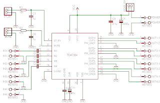

I didn’t find much information about this chip on the internet so I decided to built it and try on my own. As datasheets of TDA7384 says it is low distortion, low output noise, low external component count. Also has Stand-By function and Mute function. It has several protections like from output short circuit to GND or to Vs, capable to handle very inductive loads, thermal limiter, load dump voltage. TDA7384 is an AB power amplifier cased in flexiwatt25 (eagle library is included in project archive) package wich is designed for high end car radio applications. It allows rail to rail output voltage swing with no need of boot-strap capacitors.

Schematics TDA7384
Schematics TDA7384


I have followed the schematic in datasheed when building circuit. In datasheet you may also find PCB layout but it is two layered and didn’t fit to may box I’ve chosen. So I have made single sided PCB 50X100mm.


PCB TDA7384 amplifier

As I put pins on PCB for ST-BY and Mute but I not using them, I connected these pins to VCC like it is shown in PCB view. According to datasheet St-By and Mute turns off amplifier if signal in input is lower than 3.5V. So it is recommended to connect these pins to Vcc if not used.
Maximum power dissipation of chip is 80W(Tcase=70ºC), so it can handle 4 channels working at power of 20W each. But of course chip in a box doesn’t have good ventilation so I’ve put a radiator to ensure that amplifier effectively dissipates heats. I didn’t try to load amplifier to maximum to se if it doesn’t heat up to much. But at normal sound level it stays warm what is normal.


On box amplifier
On box amplifier


Dont forget to put thermal paste between chip and radiator to ensure lower thermal resistance. And here we go – brand new power amplifier ready to go:


TDA7384 Already to use
Already to use


source: [link]

Readmore → TDA7384 4 x 22W car power amplifier

Doubler Digital Frequency circuit


Doubler Digital Frequency circuit includes a simple and easy to understand. Digital Frequency Doubler circuit application contained in the system electronics such as audio-producing organ, or keyboard. The function of this series Digital Frequency Doubler for multiplying two input frequencies.

The process of multiplying 2 on scales in an organ in principle is like this series Digital Frequency Doubler. Example of rising to a ringing tone DO RE then electronically technique in it is by multiplying the two frequency bands such as this series Digital Frequency Doubler.
Digital Frequency Doubler.

Readmore → Doubler Digital Frequency circuit

Communication between Mitsubishi FX3U PLC and SCADA via RS485BD


Hi Friends, Here i want share with you a tutorial on how to establish Communication between Mitsubishi FX3U PLC and Elipse SCADA via RS485 BD 


The required Items for the setup is as follows


Sr. no.
Material
1
PLC Type : FX Series
2
CPU      : FX3U
3
Module   : FX3U RS485BD
4
SCADA Make : Elipse
5
SCADA Type : 20/300/ Unlimited Tags
6
Other


Figure Connection between PC(SCADA) & PLC(FX3U)


 The required cables are as follows


Sr. no.
Item
Description
1
Medoc cable
(MITSU-CAB2A)
Prog. cable for FX PLC
2
Converter Cables
*1
Comm. Cable for PC ,PLC &
Converter

 *1 To connect the SCADA to the controller the RS 232 to RS 485 Converter  is used. The Converter is having RS422/485 port for connecting to PLC & RS232 port on other side for connection to PC.


As the FX-485BD Port is used, PLC parameter settings are required on PLC side.
PLC Parameter Configuration for Channel1:
1. Baud Rate: 9600.
2. Data Bits: 7 bits
3. Parity : Even
4. Stop Bit: 1 bit
5. Sum Check: Yes
6. Transmission Control: Without CR, LF
7. H/W Type: RS485
8. Station No.: 01
PLC Communication Parameter Settings using GX Developer:

PLC Communication Parameter Settings using GX Developer

 SCADA Program settings


 SCADA Driver Details:


Driver
MELSEC-A.dll
Version
1.02
Latest Update
2004.10.20
Driver Help
Melsec-A_US.pdf


Driver Setting Parameters:
P1: 1 (Comm. Port)
P2: 3721(Comm. Parameters: 9600 bps, 7 data bits, Even
Parity & 1 stop bit)
P3: 300 (Timeout in milliseconds)
P4: 10 (For RS485)
Other needed Configuration is done through “Extra  Configuration “Dialog as follows:


• Snap shot of Driver Settings in Elipse SCADA software
 

Step 1: Enter the Driver Parameters P1-P4.


Driver Parameters
Step 2: Click on “Extra” button to edit settings.


 Step3: In “Extra” menu select “Protocol” option to edit Protocol  Settings.


“Protocol” option

 Tag Addressing Parameters:
 

The Tags are generated by using N1-N4 parameter settings as follows:
 

N1: Station Number (e.g.: 1)

N2: CPU Number (normally 255)

N3: Variable Type (e.g.: 14 for D Register)

N4: Variable Address (e.g.:10 for D10 Register)

Scan: User Defined
 

• Snap shot of Tag Addressing Parameters in Software
 
Tag Addressing Parameters

If you like the this Tutorial on PLC please Share this.
 

Readmore → Communication between Mitsubishi FX3U PLC and SCADA via RS485BD

Wednesday 25 January 2017

Power amplifier circuit 60 W mono


Wow this is nice intregated amplifier circuit , because this IC can be power output up to 60 Watt . With minimum require voltage 8 V , and maximum voltage 35 V . But this circuit is'nt so good to working on car , because output sound is very loud but not smooth. Amplifier so good working on full range , with speaker full range 100W and impedance 8 Ohm.
Below it is schematic :


Click to view large

The circuit above use IC AN7170 , the original output power IC is 20 W with impedance. But with use the circuit output elevated up to 60W.

Readmore → Power amplifier circuit 60 W mono

Easy 6V Fluorescent Light


 A fluorescent lamp or else fluorescent tube is a gab-discharge lamp with the aim of uses electricity to excite mercury vapor. The excited mercury atoms bring into being squat-wave ultraviolet light to facilitate subsequently causes a phosphor to fluoresce, producing visible light. The following schematic shows a easy 6V Fluorescent Light Circuit Diagram design.

easy 6V Fluorescent Light Circuit Diagram design
Simple 6V Fluorescent Light Circuit Diagram design

Readmore → Easy 6V Fluorescent Light

35W 4 Channel Amplifier for car audio AN7555NZ


35W 4-Channel Amplifier for car audio
Datasheet for AN7555NZ: Download
Readmore → 35W 4 Channel Amplifier for car audio AN7555NZ

Tuesday 24 January 2017

MP3 Car Amplifier Schematic Circuits 150W


MP3 Car Amplifier Schematic Circuits 150W MP3 Car Amplifier Schematic Circuits 150W
These accessories are low cost, aerial speed, bifold JFET ascribe operational amplifiers with an internally akin ascribe account voltage (BI-FET II technology). They crave low accumulation accepted yet advance a ample accretion bandage amplitude artefact and fast bulk rate. In addition, able-bodied akin aerial voltage JFET ascribe accessories accommodate actual low ascribe bent and account currents. The LF353 is pin accordant with the accepted LM1558 acceptance designers to anon advancement e the all-embracing achievement of absolute LM1558 and LM358 designs. These amplifiers may be acclimated in applications such as aerial acceleration integrators, fast D/A converters, sample and authority circuits and abounding added circuits acute low ascribe account voltage, low ascribe bent current, aerial ascribe impedance, aerial bulk amount and advanced bandwidth. The accessories additionally display low babble and account voltage drift. (National Semiconductor

Internally trimmed offset voltage: 10 mV
Low input bias current: 50pA
Low input noise voltage: 25 nV
Low input noise current: 0.01 pA
Wide gain bandwidth: 4 MHz
High slew rate: 13 V/us
Low supply current: 3.6 m
High input impedance: 1012.
Low total harmonic distortion : <>

Readmore → MP3 Car Amplifier Schematic Circuits 150W

Solar LED Lantern Circuit Diagram


This solar LED lantern can be used as an emergency light. Its 6V battery can be charged either from 230V, 50Hz AC mains or a 12V, 10W solar panel. Two LED indicators have been provided—red LED (LED1) indicates battery charging and green LED (LED2) indicates fully-charged battery.


Solar LED Lantern Circuit Diagram


You can choose to charge the battery either from the mains power or the solar panel by using the single-pole, double-throw (SPDT) switch. Capacitor C1 (1000µF, 35V) removes ripples from the power supply and regulator IC LM7809 (IC1) provides regulated 9V DC to the emitter of pnp transistor T1 (TIP127/BD140) and pin 7 of op-amp IC CA3140 (IC2), which is configured in comparator mode.

The reference voltage of 6.3V at pin 2 of IC2 is obtained through the combination of resistor R7 (1-kilo-ohm) and zener diode ZD1 (6.3V). The comparator controls charging of the battery. Pin 3 of IC2 is connected to the positive terminal of the battery to be charged through resistor R5. When the battery is fully charged, it stops charging and the green LED (LED2) glows to indicate the full-charge status.

When the battery voltage is low, diode D1 (1N4007) forward-biases and the battery connects (through resistor R3) to the collector of T1 for charging (indicated by the glowing of red LED1). Three high-wattage white LEDs (LED3 through LED5), such as KLHP3433 from Kwality Photonics, are used for lighting. These are switched on using switch S3.

Readmore → Solar LED Lantern Circuit Diagram

A Good Auto Sound System is a Requirement not a Luxury


How do you decide which auto sound system is best for you? This is a question that many consumers ask in the U. S. each and every day. The truth is that only you can decide what kind of sound you find enjoyable and what you are seeking in the sound system you will ultimately purchase. A good sound system will greatly improve how you feel about not only the vehicle you drive but also your disposition after your daily commute. It may seem like such a small thing, the changing of a sound system, but it does seem to have such a profound impact on how we start our days. Of course we all know that getting your day off to a good start sets the tone for the entire day and if that day is Monday it sets the tone for not only the day ahead but also the week to come.


Music affects almost every aspect of our lives. Most of us do not realize the impact that music has on our day-to-day lives and it is quite difficult because our world seems to be filled with it. It is much easier however, to explain the difference a good sound system makes. It's funny, I find myself in a hurry to get out of stores that have lousy sound systems and speakers that dribble out little more than static while I can shop for hours in a store that has tasteful music playing in the background over a good sound system. I prefer the volume lower and the music playing in the background rather than being the center of my attention.

Most of us find that soft music playing in the background is rather unobtrusive and allows us to get along with our thoughts and the mission at hand while loud music blaring over antiquated speakers does a great deal to disrupt our thought processes which will only serve to send us along to the next errand on our list. If you'll notice it seems that clerks in the stores where the loud music blares along are often not as even tempered as those in stores that play music at respectful volumes and have very well kept sound systems. I think I would be cranky too after listening to music in a manner that music wasn't meant to be heard.

I'm not a music snob by any means; I simply enjoy listening to music for the sake of actually hearing the music. Loud music is good sometimes but not when I have other things on my mind. I prefer that music remain in the background when I'm running about taking care of errands, even in the car. The hallmark of a good auto sound system is that it sounds good even at low volumes. This means you can enjoy music in the background, hum along, or simply ignore the music in favor of the action taking place on the road.

The point I'm trying to make is that even though you may not realize the impact that a good auto sound system has on music immediately, you will definitely feel the difference it makes over time. The better the sound system, the better the sound and music is after all, sound.

If you are a true lover of music and spend a great deal of your week or even any given day in your vehicle, doesn't it make sense to invest heavily in your auto sound system? I know for me that particular decision is a no brainer. I love music and it is an important part of not only my life but also the lives of my children. As a result we spend a lot of time listening to the radio in our SUV and singing along. Even when we aren't listening to music, I enjoy listening talk radio and the news on NPR. These things are an important part of my day and I really enjoy all that each and every one adds to my life. Because of that, I find my investment in a good auto sound system to be a requirement rather than a luxury.


Readmore → A Good Auto Sound System is a Requirement not a Luxury

LM1875 20 Watt Audio Power Amplifier


20 Watt amplifier
20 Watts Power Amplifier circuit can be made ​​with an IC power amplifier LM1875. IC LM1875 is a single chip power amplifier from National. 20 watts audio amplifier with LM1875 is a low power amplifier with good quality to the room.


To assemble the amplifier 20 watts with IC LM1875 component is not needed much support. 20 watts power amplifier using LM1875 IC in this article using symmetrical power supply. The virvuit of 20 watts audio power amplifier with IC LM1875 can be used as an experiment or first project for the reader, because it is simple and assembly of high success.

LM1875 | 20 Watt Audio Power Amplifier
Schematic Amplifier LM1875

LM1875 amplifier circuit with the above may result in the strengthening of the voltage up to 27dB for each channel (1 channel 1 IC). Strengthening the voltage can be changed by changing the feedback that is R5 R (on the circuit above using R 22K). But the tension reinforcement can not be less than 20 dB because it can cause oscillation. For the power supply or power supply 20 watts power amplifier rngakaian with lm1875 can use travo 2-3A with CT.

Readmore → LM1875 20 Watt Audio Power Amplifier

33KV substation with two 40 MVA 132 33KV transformers


Readmore → 33KV substation with two 40 MVA 132 33KV transformers

Monday 23 January 2017

Solar Powered SLA Battery Maintenance


This circuit was designed to ‘baby-sit’ SLA (sealed lead-acid or ‘gel’) batteries using freely available solar power. SLA batteries suffer from relatively high internal energy loss which is not normally a problem until you go on holidays and disconnect them from their trickle current charger. In some cases, the absence of trickle charging current may cause SLA batteries to go completely flat within a few weeks. The circuit shown here is intended to prevent this from happening. Two 3-volt solar panels, each shunted by a diode to bypass them when no electricity is generated, power a MAX762 step-up voltage converter IC. 


Solar Powered SLA Battery-Maintenance-Circuit-Diagram
Solar Powered SLA Battery Maintenance Circuit Diagram

The ‘762 is the 15-volt-out version of the perhaps more familiar MAX761 (12 V out) and is used here to boost 6 V to 15 V.C1 and C2 are decoupling capacitors that suppress high and low frequency spurious components produced by the switch-mode regulator IC. Using Schottky diode D3, energy is stored in inductor L1 in the form of a magnetic field. When pin 7 of IC1 is open-circuited by the internal switching signal, the stored energy is diverted to the 15-volt output of the circuit. The V+ (sense) input of the MAX762, pin 8, is used to maintain the output voltage at 15 V. C4 and C5 serve to keep the ripple on the output voltage as small as possible. R1, LED D4 and pushbutton S1 allow you to check the presence of the 15-V output voltage.

D5 and D6 reduce the 15-volts to about 13.6 V which is a frequently quoted nominal standby trickle charging voltage for SLA batteries. This corresponds well with the IC’s maximum, internally limited, output current of about 120 mA. The value of inductor L1 is not critical — 22 µH or 47 µH will also work fine. The coil has to be rated at 1 A though in view of the peak current through it. The switching frequency is about 300 kHz. A suggestion for a practical coil is type M from the WEPD series supplied by Würth (www.we-online.com). Remarkably, Würth supply one-off inductors to individual customers. At the time of writing, it was possible, under certain conditions, to obtain samples, or order small quantities, of the MAX762 IC through the Maxim website at www.maxim-ic.com.
Author : Myo Min

Readmore → Solar Powered SLA Battery Maintenance

Sunday 22 January 2017

zBot 10 A Power Stage for DC Motor Circuit Diagram


zBot :10-A Power Stage for DC Motor Circuit Diagram . If you look at the chassis of the zBot vehicle1, you’ll find two parts requiring intelligent control: the steering servo and the DC motor. The so called H-bridge is the normal circuit for electronic control of revolution speed and direction. The DC motor of a Tamiya car is powerful enough to propel zBot at up to 20 miles per hour.
.
The motor then consumes more than 10 A, so we choose high-current power MOSFETs for the driver stage. There are lots of different devices to choose from. The MOSFET we require has to supply the maximum motor current and, importantly, it has to be switched with gate voltages of about 5 V. In this case, the microcontroller switches the power stage (‘low side’) directly. For high side driving level shifters are necessary. The schematic of the H-bridge power stage shows a few inverters, NAND gates and two tri-stateable drivers. These logic functions are very important as the easier way, i.e.., directly controlling all four MOSFET has a fatal disadvantage.

zBot :10-A Power Stage for DC Motor Circuit Diagram

zBot :10-A Power Stage for DC Motor Circuit Diagram


In case of a software crash it could happen that two ore more MOSFETs are switched on incor-rectly for exam-ple, T4 and T7. In that case, the current through the transistors is limited by the internal resistors of the MOSFETs (about 10 mO) only. Such a fatal error would destroy the MOSFETs. The logic functions configured here effectively avoid illegal states.To control the DC motor, three signals are needed: DIR, PWM and STOP. DIR controls the direction of the motor revolution, PWM the speed, and STOP brakes the motor.

The software module for the DC motor is called dcm.c.(070172-I) The complete document called Zbot  the Robot Experimental Platform is available for free downloading from the Elektor Electronics website. The file number is 070172-11.zip (July/August 2007).

Sourced by : Circuitsstream.blogspot.com

Readmore → zBot 10 A Power Stage for DC Motor Circuit Diagram

How to make a guitar cable


Today we're going to do a quick run through of how to make a guitar cable. It’s a pretty simple procedure, but if you’ve never made one before, it can be a little bit daunting at first.

To make a cable, you will need to following items:
  1. Some cable
  2. Two ¼” jack plugs
And the following tools:
  1. A soldering iron and some solder
  2. Wire cutters/strippers/pliers
 Here’s the cable we're going to use:


 And we're going to use two of these jack plugs:


I really like this design of plug (and I’ve used a tonne of different ones over the years). To open it, you unscrew the end cap/cable relief:

 
Then lift up the cover:


 Which reveals the following:

 
Obviously you can use a different design if you like.

Today we're making a short cable that will go between effects pedals. There’s nothing different between this sort of cable and a standard guitar cable, apart from the length.

This one, we're going to cut to 20cm (8”):


Then trim the outer sleeve back by 15mm (a little under 5/8”):


We trim the inner wire insulation back by a few mm and then twist the end of the wire together. The outer shielding wiring is also gathered and twisted together:


All of this is done at both ends, leaving us with this:


We then slide any necessary items over the cable before doing any soldering. You’ll get away with forgetting this for the first plug, since you can always slide it on from the other end after soldering. However, for the second plug, it’ll be too late and you’ll have to unsolder something to fix it. 


Next step is to melt a couple of healthy blobs of solder onto the two positions where we intend to attach wires.


Then we “tin” the wires, which is to say, we melt a little bit of solder onto them:


We're also going to cut the outer ground wire a little shorter, so that it fits its position on the plug better:

 
Now we solder the wires on. When doing this, try not to keep the soldering iron on the plug for an extended amount of time, as some of them can be ruined very easily.

Firstly, the ground wire:

And then the positive/tip wire:


Before closing up, we need to secure the cable by tightening the metal clamp as follows:


Then we place the cover back in place:


And tighten the end plug/cable relief:


We do the same for the other end of the cable:


And here’s the end result:


Readmore → How to make a guitar cable