Showing posts with label timer. Show all posts
Showing posts with label timer. Show all posts
Sunday, 19 March 2017
PIC16F887 877 programming in C Tutorial 3 3 Timer 2
Timer 2:
Timer2 is an 8-bit timer with a prescaler and a postscaler. It can be used as the PWM time base for the PWM mode of the CCP module(s). The TMR2 register is readable and writable and is cleared on any device Reset.
The input clock (FOSC/4) has a prescale option of 1:1, 1:4 or 1:16, selected by control bits T2CKPS1:T2CKPS0 (T2CON<1:0>).
The Timer2 module has an 8-bit period register, PR2.
Timer2 increments from 00h until it matches PR2 and then resets to 00h on the next increment cycle. PR2 is a readable and writable register. The PR2 register is initialized to FFh upon Reset.
Timer2 increments from 00h until it matches PR2 and then resets to 00h on the next increment cycle. PR2 is a readable and writable register. The PR2 register is initialized to FFh upon Reset.
The match output of TMR2 goes through a 4-bit postscaler (which gives a 1:1 to 1:16 scaling inclusive) to generate a TMR2 interrupt (latched in flag bit, TMR2IF (PIR1<1>)).
Timer2 can be shut-off by clearing control bit, TMR2ON (T2CON<2>), to minimize power consumption.
Timer2 can be shut-off by clearing control bit, TMR2ON (T2CON<2>), to minimize power consumption.
Prescaler and Postscaler - Timer2 is an 8-bit timer with a prescaler and a postscaler. Each allows to make additional division of the frequency clock source.
Prescaler divides the frequency clock source BEFORE the counting take place at the register TMR2, thus the counting inside the TMR2 register is performed based on the divided frequency clock source by the Prescaler.
Prescaler divides the frequency clock source BEFORE the counting take place at the register TMR2, thus the counting inside the TMR2 register is performed based on the divided frequency clock source by the Prescaler.
Postscaler divides the frequency that comes out of the Comparator.
T2CON Register:

How to calculate the required values of the TIMER2: 
Fout – The output frequency after the division. Tout – The Cycle Time after the division.
4 - The division of the original clock by 4, when using internal crystal as clock (and not external oscillator).
Count - A numeric value to be placed to obtain the desired output frequency - fout.
(PR2 – TMR2) - The number of times the counter will count.
Code:
Lets write the code to toggle the bits of portc after 2 sec;
void main() {
// using 4MHz ext xtal
int count=0;
trisc=0;
// using 4MHz ext xtal
int count=0;
trisc=0;
portc=255;
/////////////////// comment this block if you are using 877///////////
ansel=0;
anselh=0;
c1on_bit=0;
c2on_bit=0;
ansel=0;
anselh=0;
c1on_bit=0;
c2on_bit=0;
////////////////////////////////////////////
t2con=124; //prescaler is 16
pr2=255; //final value to count
tmr2=0; //initial value
while(1){
t2con=124; //prescaler is 16
pr2=255; //final value to count
tmr2=0; //initial value
while(1){
while(!tmr2if_bit); //tmr2 flag bit
tmr2if_bit=0;
cnt++;
if(cnt==488){ //for 2 sec(16*256u*488=2sec)
portc=~portc;
cnt=0;
}
}
}
tmr2if_bit=0;
cnt++;
if(cnt==488){ //for 2 sec(16*256u*488=2sec)
portc=~portc;
cnt=0;
}
}
}
Schematic:
Timer 0 schematic can be used (tutorial 3 part 1).

Sunday, 5 March 2017
A Bedside Lamp Timer Circuit Diagram
Description
 Parts:
Circuit operation:
The purpose of this circuit is to power a lamp or other appliance for a given time (30 minutes in this case), and then to turn it off. It is useful when reading at bed by night, turning off the bedside lamp automatically in case the reader falls asleep... After turn-on by P1 pushbutton, the LED illuminates for around 25 minutes, but then it starts to blink for two minutes, stops blinking for two minutes and blinks for another two just before switching the lamp off, thus signaling that the on-time is ending. If the user want to prolong the reading, he/she can earn another half-hour of light by pushing on P1. Turning-off the lamp at user's ease is obtained by pushing on P2.
Circuit diagram: - R1 = 1K
- R2 = 4K7
- R3 = 10M
- R4 = 1M
- R5 = 10K
- C1 = 470µF-25V
- C2-C4100nF-63V
- C1 = 470µF-25V
- C2-C4 = 100nF-63V
- D1-D4 = 1N4002
- D5 = 5mm. Red LED
- IC1 = CD4012
- IC2 = CD4060
- Q1 = BC328
- Q2 = BC547
- P1,P2 = SPST Pushbuttons
- T1 = 9+9 Volt Secondary 1VA Mains transformer
- RL1 = 10.5V 470 Ohm Relay with SPDT 2A 220V switch
- PL1 = Male Mains plug
- SK1 = Female Mains socket
Q1 and Q2 form an ALL-ON ALL-OFF circuit that in the off state draws no significant current. P1 starts the circuit, the relay is turned on and the two ICs are powered. The lamp is powered by the relay switch, and IC2 is reset with a positive voltage at pin 12. IC2 starts oscillating at a frequency set by R4 and C4. With the values shown, pin 3 goes high after around 30 minutes, turning off the circuit via C3. During the c6 minutes preceding turn-off.
The LED does a blinking action by connections of IC1 to pins 1, 2 & 15 of IC2. Blinking frequency is provided by IC2 oscillator at pin 9. The two gates of IC1 are wired in parallel to source more current. If required, a piezo sounder can be connected to pins 1 & 14 of IC1. Obviously, timings can be varied changing C4 and/or R4 values.
Source - http://www.extremecircuits.net/2009/12/bedside-lamp-timer-circuit-schematic.html
Thursday, 16 February 2017
Simple LED flasher circuit using NE555 timer IC
This circuit consumes more power, but it's advantage is when you need a variable flash rate, like for strobe circuits. You can actually use this circuit as a remote control for strobes that have a remote input. Of course, it has many other applications besides strobes.

- R1, R2, C1 and the supply voltage determine the flash rate. Using a regulated power supply will do much to insure a stable flash rate. For a variable flash rate, replace R1 with a 1 megohm pot in series with a 22k resistor.
- The duty cycle of the circuit (the percentage of the time LED 1 is on to the time it is off during each cycle) is deterimed by the ratio of R1 to R2. If the value of R1 is low in relationship to R2, the duty cycle will be near 50 percent. If you use both LEDs, you will probably want a 50 percent duty cycle. On the other hand, if R2 is low compared to R1, the duty cycle will be less than 50 percent. This is useful to conserve battery life, or to produce a strobe type effect, when only LED1 is used.
- The NE555 timer chip can be damaged by reverse polarity voltage being applied to it. You can make the circuit goof proof by placing a diode in series with one of the supply leads.
- The purpose of R3 and R4 is to limit current through the LEDs to the maximum they can handle (usually 20 milliamps). You should select the value of these according to the supply voltage. 470 ohms works well with a supply voltage of 9-12 volts. You will need to reduce the value for lower supply voltages.
- Rainbow Kits offers several kits to build the above circuit. You can also order these kits from RadioShack.com. The Radio Shack catalog numbers (and web pages) are as follows: standard kit with two 5mm red LEDs, (990-0067), kit with two red, two green and two yellow 3mm LEDs, (990-0063), kit with jumbo green LEDs, (990-0048), kit with jumbo red LEDs, (990-0049). You can also buy all the parts to build the circuit at your local Radio Shack store, including a circuit board (276-159B).
I have built a miniature strobe circuit as follows. Use a 250k pot in series with a 4.7k resistor for R1. The 4.7k resistor sets the upper flash rate limit. Use 2.2k for R2. That sets a really short duty cycle. For this circuit, you don't use LED 2 or R4. For LED 1, I used a two Radio Shack white LEDs in series and no R-3. The circuit runs on a 9 v battery. link
Monday, 13 February 2017
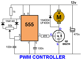
PWM Controller 555 timer circuits
Saturday, 4 February 2017
Auto Burglar Alarm Using 555 Timer ICs
This electronic circuit project using two 555 timer ICs, Simple circuit and low-cost circuit diagram, basic circuit could be used for a home also. The circuit Auto burglar alarm will sound your car horn if anyone opens the car door while the circuit is armed. The timers will allow you to leave the car without sounding the horn. To turn the circuit on S1 must be closed.
Auto Burglar Alarm Circuit Diagram:

To set the alarm, open S2 (it is normally closed ) this will give you about 5 seconds to get out and close the door. The exit delay time is set by R1 and C1. If anyone opens the doors for more than two seconds the horn will sound until power is removed from the circuit. The 2 second time is set by R2 and C2. If you open the door, you must deactivate the alarm by closing S2.
Auto Burglar Alarm Circuit Diagram:
To set the alarm, open S2 (it is normally closed ) this will give you about 5 seconds to get out and close the door. The exit delay time is set by R1 and C1. If anyone opens the doors for more than two seconds the horn will sound until power is removed from the circuit. The 2 second time is set by R2 and C2. If you open the door, you must deactivate the alarm by closing S2.
Thursday, 2 February 2017
Simple IC 555 Timer Tester Circuit Diagram
This is a Simple IC 555 Timer Tester Circuit Diagram. This simple and easy-to-use gadget not only tests the IC 555 timer in all its basic configurations but also tests the functionality of each pin of the timer. Once a timer is declared fit by this gadget, it will function satisfactorily in whatever mode or configuration you may try it. The two basic configurations in which a timer IC 555 can be used are the astable and the monostable modes of operation.
When the DPDT switch (S2) is in position 1-1, the timer under test automatically gets wired as a monostable multivibrator. In this case, the monoshot can be triggered by the microswitch (S1). The debouncing circuit constituted by the two NAND gates of IC1 (N1 and N2) produces a clean rectangular pulse when the microswitch is pressed. Resistor R3, capacitor C1 and diode D1 ensure that the trigger terminal of timer IC 555 (pin 2 is the trigger terminal) gets the desired positive-to-ground trigger pulse. This differentiator circuit also ensures that the width of the trigger pulse is less than the expected monoshot output pulse.
Simple IC 555 Timer Tester Circuit Diagram

The monoshot output pulse width is a function of the series combination of resistor R8 and potentiometer VR2, and capacitor C4. When DPDT switch S2 is in position 2-2, the timer gets configured for the astable mode of operation. The output is a pulse train with the high time period determined by the series combination of resistors R8, potentiometer VR2, resistor R9 and capacitor C4, whereas the low time period is determined by resistor R9 and capacitor C4.
The reset terminal of timer IC (pin 4) should be tied to Vcc normally. More precisely, the voltage at pin 4 should be greater than 0.8V. A voltage less than that resets the output. Whether you have connected the timer in the monoshot or astable mode of operation, the output goes low the moment you bring the reset terminal below 0.8V.
The control terminal (pin 5) can be used to change the high time (‘on’ time) of the output pulse train in the astable mode and the output pulse width in the monoshot mode by applying an external voltage. This external voltage basically changes the reference voltage levels of the comparators inside the IC. The levels are set by three identical resistors of usually 5 kilo-ohms inside the IC connected from Vcc to ground, at 2/3Vcc for pin 5 and 1/3Vcc for pin 2. These levels can be changed by connecting an external resistor between pin 5 and ground. Resistor R10 and potentiometer VR3 have been connected for this purpose.
The pulse width in the monoshotmode is given by:
1.1×total charging resistance×charging capacitance
This expression is valid when there is no external resistor connected at pin 5. The pulse width can be reduced by connecting an external resistor.
The high and low time periods in the astable mode are:
High time period = 0.69×chargingresistance×charging capacitance
Low time period = 0.69×dischargeresistance×capacitance
Again the expressions are true with no external resistor at pin 5. The high time period can be made to decrease by connecting an external resistor between pin 5 and ground.
The circuit can thus be used to check:
1. The timer IC in astable configuration.
2. The timer IC in monostable configuration.
3. The capability of the reset terminal to override all functions and rest the output to low.
4. The function of the control terminal to change the ‘on’ or the ‘high’ time of the output waveform in astable mode of operation and the output pulse width in monostable mode of operation.
The circuit operates off a 9V battery, which makes the gadget portable. You can construct it easily on any general-purpose PCB along with the 8-pin socket.
To test an IC 555:
1. Insert it into the socket.
2. Set switch S2 in position 1-1.
3. Switch on the power supply by flipping switch S3 to ‘on’ position. Power-indicator LED (LED3) glows to indicate that the circuit is ready to test the IC timer.
4. If the IC is okay, LED1 glows because the IC is wired as a monoshot and in the absence of any trigger, its output is low.
5. Apply the trigger pulse by momentarily pressing switch S1. LED1 stops glowing and, in turn, LED2 glows. This confirms that the output of the monoshot has gone high. After the predetermined time period, LED2 goes off and LED1 again glows. Vary preset VR2 and trigger the monoshot again through switch S1. You will find that LED2 glows this time for a longer or a smaller time period depending upon whether you increased or decreased VR2 resistance.
6. For checking the reset function of the timer, trigger the monoshot again, and before the expected time is over, quickly decrease the potmeter VR1 resistance so as to bring the voltage at pin 4 below 0.8V. You will observe the output going low (indicated by glowing LED1 and extinguished LED2).
7. For checking the control function of the timer IC, set potmeter VR1 again in the maximum resistance position. Also set preset VR3 in the minimum resistance position. Trigger the monoshot using switch S1. You’ll observe its output going high for a time period that is much less than that determined from the series combination of R8 and VR2, and capacitor C4. In fact, for any fixed setting of this series combination, the output pulse width can be observed to vary for different values of potmeter VR3 resistance—by triggering the monoshot several times, once for each setting of VR3.
8. Now set the DPDT switch in position 2-2. LED1 and LED2 glow alternatively with the timing determined by the resistances in the charge and discharge paths. This means the timer IC is okay and wired in astable mode.
9. The functions of reset and control pins can be checked in astable configuration too in the same way as discussed above for the monoshot configuration.
The reset terminal of timer IC (pin 4) should be tied to Vcc normally. More precisely, the voltage at pin 4 should be greater than 0.8V. A voltage less than that resets the output. Whether you have connected the timer in the monoshot or astable mode of operation, the output goes low the moment you bring the reset terminal below 0.8V.
The control terminal (pin 5) can be used to change the high time (‘on’ time) of the output pulse train in the astable mode and the output pulse width in the monoshot mode by applying an external voltage. This external voltage basically changes the reference voltage levels of the comparators inside the IC. The levels are set by three identical resistors of usually 5 kilo-ohms inside the IC connected from Vcc to ground, at 2/3Vcc for pin 5 and 1/3Vcc for pin 2. These levels can be changed by connecting an external resistor between pin 5 and ground. Resistor R10 and potentiometer VR3 have been connected for this purpose.
The pulse width in the monoshotmode is given by:
1.1×total charging resistance×charging capacitance
This expression is valid when there is no external resistor connected at pin 5. The pulse width can be reduced by connecting an external resistor.
The high and low time periods in the astable mode are:
High time period = 0.69×chargingresistance×charging capacitance
Low time period = 0.69×dischargeresistance×capacitance
Again the expressions are true with no external resistor at pin 5. The high time period can be made to decrease by connecting an external resistor between pin 5 and ground.
The circuit can thus be used to check:
1. The timer IC in astable configuration.
2. The timer IC in monostable configuration.
3. The capability of the reset terminal to override all functions and rest the output to low.
4. The function of the control terminal to change the ‘on’ or the ‘high’ time of the output waveform in astable mode of operation and the output pulse width in monostable mode of operation.
The circuit operates off a 9V battery, which makes the gadget portable. You can construct it easily on any general-purpose PCB along with the 8-pin socket.
To test an IC 555:
1. Insert it into the socket.
2. Set switch S2 in position 1-1.
3. Switch on the power supply by flipping switch S3 to ‘on’ position. Power-indicator LED (LED3) glows to indicate that the circuit is ready to test the IC timer.
4. If the IC is okay, LED1 glows because the IC is wired as a monoshot and in the absence of any trigger, its output is low.
5. Apply the trigger pulse by momentarily pressing switch S1. LED1 stops glowing and, in turn, LED2 glows. This confirms that the output of the monoshot has gone high. After the predetermined time period, LED2 goes off and LED1 again glows. Vary preset VR2 and trigger the monoshot again through switch S1. You will find that LED2 glows this time for a longer or a smaller time period depending upon whether you increased or decreased VR2 resistance.
6. For checking the reset function of the timer, trigger the monoshot again, and before the expected time is over, quickly decrease the potmeter VR1 resistance so as to bring the voltage at pin 4 below 0.8V. You will observe the output going low (indicated by glowing LED1 and extinguished LED2).
7. For checking the control function of the timer IC, set potmeter VR1 again in the maximum resistance position. Also set preset VR3 in the minimum resistance position. Trigger the monoshot using switch S1. You’ll observe its output going high for a time period that is much less than that determined from the series combination of R8 and VR2, and capacitor C4. In fact, for any fixed setting of this series combination, the output pulse width can be observed to vary for different values of potmeter VR3 resistance—by triggering the monoshot several times, once for each setting of VR3.
8. Now set the DPDT switch in position 2-2. LED1 and LED2 glow alternatively with the timing determined by the resistances in the charge and discharge paths. This means the timer IC is okay and wired in astable mode.
9. The functions of reset and control pins can be checked in astable configuration too in the same way as discussed above for the monoshot configuration.
Sourced By: EFY. Author: Raj K. Gorkhali
Saturday, 28 January 2017
Simple Timer with Transistor Circuit Diagram
The below Simple Timer with Transistor Circuit Diagram is a simple timer that uses only two Darlington transistors and a capacitor base to generate a delay. When SW1 is pressed, the timer starts, the time setting is set by VR1. The duration of the timer is given by the values of the potentiometer VR1 and the capacitor C1 that this circuit is 220 pF. To reach other durations of time must change the values of these two components.
Timer with Transistor Circuit Diagram

Sunday, 8 January 2017
Transistor As a timer circuit
Basically on all timer or timer circuit utilizing most of the basic characteristics of the capacitor.

The basic characteristic is the process of filling and discharge that occurs in the capacitor. The length of time charging and release depends on the value of the capacitor.
If we observe the above circuit, the light will immediately switch SW1 turns on when we plug it into potensio VR1, this is because the current flowing from VR1 to trigger the transistor base should fill the first capacitor C1. Semakian large capacitance value of C1 then the longer the time required by the transistor to turn on the lights. Then if we connect it to the Ground SW1 then light would soon die and the capacitor will immediately clear the cargo. So can we draw the conclusion that the transistor can be used as a timer circuit using capacitor charging and discharging properties.
Wednesday, 4 January 2017
Inverter as High Voltage Low Current Source Using by 555 timer
This is a simple Electronic Circuit Projects of Inverter as high voltage low current source using by 555 timer IC. The circuit is capable of providing power for portable Geiger counters, dosimeter chargers, high resistance meters, etc.
Inverter as High Voltage Low Current Source Circuit Diagram:

The 555 timer IC is used in its multivibrator mode, the frequency adjusted to optimize the transformer characteristics. When the output of the IC is high, current flows through the limiting resistor, the primary coil to charge C3. When the output is low, the current is reversed With a suitable choice of frequency and C3, a good symmetric output is sustained.
Inverter as High Voltage Low Current Source Circuit Diagram:
The 555 timer IC is used in its multivibrator mode, the frequency adjusted to optimize the transformer characteristics. When the output of the IC is high, current flows through the limiting resistor, the primary coil to charge C3. When the output is low, the current is reversed With a suitable choice of frequency and C3, a good symmetric output is sustained.
Friday, 9 December 2016
PWM Controller 555 timer circuits
Tuesday, 15 November 2016
Pulse Timer Control Relay Circuit with IC555
Today we would like to offers solutions for a set time for take control relay and take NO. / NC. contact to apply to control other devices . such as disable or enable the device.function of this circuit is using IC555 to determine the pulse and a resistor R1 to the period of time.
Pulse Timer Control Relay Circuit Diagram

R1 #Seconds
100k 2
220k 3
470k 6
1M 15
The increase provides more time to increase the value of the Capacitor.
Part List
R1 = 1 Meg, Preset Pot
R2 = 10K
R3,R4 = 1K
C1 = 10uF, 16V
C2 = 0.01uF
T1 = BC547 (Gen Purp NPN)
T2 = 2N2222 (Hi Current NPN)
D1 = 1N4001 (Gen Purp Si)
IC1 = 555 (Lo-Power version)
RLA1 = Relay, 9V (amps of your choice)
Pulse Timer Control Relay Circuit Diagram
R1 #Seconds
100k 2
220k 3
470k 6
1M 15
The increase provides more time to increase the value of the Capacitor.
Part List
R1 = 1 Meg, Preset Pot
R2 = 10K
R3,R4 = 1K
C1 = 10uF, 16V
C2 = 0.01uF
T1 = BC547 (Gen Purp NPN)
T2 = 2N2222 (Hi Current NPN)
D1 = 1N4001 (Gen Purp Si)
IC1 = 555 (Lo-Power version)
RLA1 = Relay, 9V (amps of your choice)
Monday, 14 November 2016
PCB Exposure Switch Timer V2 0
After some modifications on my UV exposure box (scanner) for better UV expose, i decided that a better pcb must me designed for switch timer. The old one had over drilled holes and it was designed and built on my very fist steps. Also the high voltage side from the low voltage wasn’t separated as it needed to be safe.

So i redesigned it in a more compact and easier to use pcb. The firmware has been also updated and now you can program the timmer by using the two buttons. The time is calculated by timer interrupt triggering using a 32.768KHz RTC Crystal with better accuracy. The display update also has been changed from static to dynamic. [ ]
Saturday, 24 September 2016
Chapter Wiring diagram light switch timer
Wiring diagram light switch timer


Wiring diagram light switch timer
Intermatic timer wiring diagram - emprendedor.link, Intermatic timer wiring diagram. need help wiring an intermatic wh40 water heater time switch into the. pool timer wiring diagram. howto wire intermatic t104 and t103.
Timers and light switch wiring - ask the electrician, Electrical question: i’m trying to replace a single pole light switch with a timer light switch in a box that also has another single pole switch going to another.
Harbor breeze ceiling fan light kit wiring diagram, Harbor breeze ceiling fan light kit wiring diagram. double ceiling fan. wiring bathroom exhaust fans with light. 3 speed ceiling fan switch wiring diagram. hunter.
# 83-87 chevy gmc fuse box diagram — circuit wiring, 83-87 chevy gmc fuse box diagram. 83-87 chevy gmc fuse box map. fuse panel layout diagram parts: radio, heater, wiper, choke heater, turn signal, power window, air.
How to run two lights from one switch : electrical online, This article and detailed wiring diagram explains how to run two lights from one switch..
Wiring a photocell for an outdoor light fixture, Electrical question: i would like control an outside light with a photo cell. wiring a 1000 watt outdoor light. the light is now wired for 240 volts and would like to.
Subscribe to:
Posts (Atom)