Wednesday, 15 February 2017
Led Flasher Type of Police Circuit Diagram
This is the simple Led Flasher Type of Police Circuit Diagram. LED flasher same as that used in the police car, where the pace at which the lights flash is well paced and there is a sequence on each side. This type of flasher is also called strobe light or stroboscopic light. I began to develop a project to be published here, but by coincidence I ended up finding a circuit, easy to build and giving effect was wanting.
The electronic circuit flasher police is a Russian site, as the Russians have their own markup for semiconductor like this project, which uses KT815 transistors, for sure you will not find these transistors in a Western store, but of course are the replacements, in this case BD135.
The electronic circuit flasher police is a Russian site, as the Russians have their own markup for semiconductor like this project, which uses KT815 transistors, for sure you will not find these transistors in a Western store, but of course are the replacements, in this case BD135.
Led Flasher Type of Police Circuit Diagram

Flasher LED Police type
This circuit is a classic of electronics, a flip-flop circuit, "astable multivibrators", this circuit is used for common flasher, but in this case two of this circuit were coupled to give the desired effect. The circuit flasher is so simple that can be done by a novice, as we see in the image below of the author, it was made on a standard printed circuit board.
How does the flasher Police
The flasher consists of two astable multivibrators, a leading astable formed by VT1 and VT2 transistors that generate the strobe and VT3 eVT4 transistors that have created short pulses to VT1 and VT2. The master oscillator is switched alternately strobe generator and the operating frequency of the generator is determined by the capacitors C1 and C4 and resistors R5, R6, R8 and R9.
You can use the trimpot R7 and R10 resistors to change the frequency of multivibrators, changing the frequency of blinking of the LEDs. The power transistors VT1 and VT3 and resistors R1 and R2 depend on the power of the LEDs used in the circuit.
Have the circuit power supply can be made with voltages 6-9 V, and its consumption is very low, enabling the use of batteries or battery. You can also change the operating voltage to 12 volts, just change some circuit resistors or put a 7809 regulator in input voltage.
Flasher LED type Police
I will give the most common equivalent found, the VT1 and VT2 transistors can be replaced by medium power transistors BD135, BD137 or BD139. The VT3 transistor can be replaced by transistors average power transistors BD136, BD138 or BD140.
But the transistor VT4 can be replaced by transistor 2sa611, BC556 or 2N4058 and other BCs of life. Below the video of the flasher police, the circuit can also be used for security systems, emergency flashing, holiday lighting, etc.
You can use higher power LEDs in this circuit since modify the resistors R1 and R2.

Booster BLW 60
In this post an opportunity, I upload booster BLW 60 which may be an inspiration to create home brew. Here I include a file layout that can be unlocked via software sprint layout. of course the software you can download here as well. ok g tuk need to talk at length, immediately wrote download the full data here

Simple Remote Control Mains Switch
As the only electronics engineer in my =family and circle of friends, it is some-times not possible to evade an appeal for help. This time the request came from a friendly elderly lady in a retirement home. In her room the light switch by the door and the pull cord above the bed operate the light fitting on the ceiling in the middle of the room. However, she would prefer that her standing lamp was operated by these switches instead, since she does not actually have a light fitting mounted on the ceiling. This standing lamp has an on/of f switch in the power cord and is plugged into a power point. However, it stands rather far from the bed so that she always has to find her way in the dark. A wireless operated power point is not really a consideration, because it is just a matter of time before the remote is lost. Or maybe not?
Remote Control Mains Switch Circuit Diagram :

Behold a feasible circuit. Buy a wireless power point and an enclosure that is big enough for the remote control and a small piece of prototyping board. On the proto-typing board build the circuit according to the accompanying schematic and (care-fully) open the remote control and solder wires to the push buttons for ‘on’ and ‘off’. Measure if these are polarised and if that is the case connect them to the 4N25 opto-couplers as shown in the schematic, where pin 5 has a higher voltage than pin 4.
The operation is as follows. The lady operates the pull cord or light switch to turn the light on. This causes the mains voltage to be applied to the transformer. The relay is activated which charges C1. While C1 charges, a small current flows through optocoupler 1. The result is that the ‘on’ button on the remote control is pressed. The remote control switches the corresponding power point on and to which the standing lamp is connected. The standing lamp will therefore now turn on. Capacitor C2 is charged at the same time. If the lady pulls the cord again, or if she operates the switch near the door, the relay will de-energise and C2 discharges across optocoupler #2. This operates the ‘off’ contact of the remote control and the light goes out.
The remote control continuous to operate from its normal battery and the white enclosure is attached to the ceiling in place of the light fitting. Diode D1 ensures that C1 is discharged when the relay de-energises. D2 ensures that C2 cannot discharge across the relay, but only across optocoupler 2.
Author : Jaap van der Graaff - Copyright :Elektor
Audio amplifier circuit with IC STK0039 good quality amplifier

Although the output of which was issued in this circuit only 35watts maximum, but th esound can be issued harsh , loud , and clear. If the voltage is fit and clean , how to assembly , components are good , the right speakers , this circuit will definitely make a sound that good to hear the ear.
See audio amplifier circuit below :

Technical Information :Vcc Max = 45VVcc TYP = 30VPo = 35WRL = 8OhmIcco TYP = 40mAIcco Max = 80mAI Max = 10A

The amplifier can use to : tuner , subwoofer surround amplifier , surround amplifier , subwoofer system , car amplifier , PC amplifier , DVD/CD amplifier , Room amplifier . Because this amplifier good quality amplifier circuit.

Monday, 13 February 2017
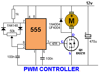
PWM Controller 555 timer circuits
Sine Wave Generation without ECCP Using single CCP Module of PIC16F877A
I had previously shown how to generate sinusoidal pulse width modulation (SPWM) signals using the ECCP module in a PIC for generating a sine wave output for use in DC-AC inverter. I have had requests from people asking how to generate the same SPWM signals with other microcontrollers that don't have the ECCP module, such as the super popular PIC16F877A.
So, here I talk about how to generate the same SPWM signals using just one CCP module as can be commonly found on so many microcontrollers. This allows much greater flexibility in microcontroller selection.
You should go through the other articles related to generating SPWM with the ECCP module (if you haven't already gone through them, that is) to get an idea of what I'm talking about regarding sine wave generation with the ECCP module and about sine wave generation in general, really:
- Generation and Implementation of Sine Wave Table
- Smart Sine - Software to generate sine table
- Generation of sine wave using SPWM in PIC16F684
- 600W 50Hz sine wave inverter test circuit
- Feedback in sine wave inverter (PIC16F series based)
- Demystifying The Use of Table Pointer in SPWM - Application in Sine Wave Inverter
The code I had previously used (utilizing the ECCP module) is:
//----------------------------------------------------------------------------------------
//Programmer: Syed Tahmid Mahbub
//Target Microcontroller: PIC16F684
//Compiler: mikroC PRO for PIC (Can easily port to any other compiler)
//-----------------------------------------------------------------------------------------
unsigned char sin_table[32]={0,25,49,73,96,118,137,
159,177,193,208,220,231,239,245,249,250,249,245,
239,231,220,208,193,177,159,137,118,96,73,49,25};
unsigned int TBL_POINTER_NEW, TBL_POINTER_OLD, TBL_POINTER_SHIFT, SET_FREQ;
unsigned int TBL_temp;
unsigned char DUTY_CYCLE;
void interrupt(){
if (TMR2IF_bit == 1){
TBL_POINTER_NEW = TBL_POINTER_OLD + SET_FREQ;
if (TBL_POINTER_NEW < TBL_POINTER_OLD){
CCP1CON.P1M1 = ~CCP1CON.P1M1; //Reverse direction of full-bridge
}
TBL_POINTER_SHIFT = TBL_POINTER_NEW >> 11;
DUTY_CYCLE = TBL_POINTER_SHIFT;
CCPR1L = sin_table[DUTY_CYCLE];
TBL_POINTER_OLD = TBL_POINTER_NEW;
TMR2IF_bit = 0;
}
}
void main() {
SET_FREQ = 410;
TBL_POINTER_SHIFT = 0;
TBL_POINTER_NEW = 0;
TBL_POINTER_OLD = 0;
DUTY_CYCLE = 0;
ANSEL = 0; //Disable ADC
CMCON0 = 7; //Disable Comparator
PR2 = 249;
TRISC = 0x3F;
CCP1CON = 0x4C;
TMR2IF_bit = 0;
T2CON = 4; //TMR2 on, prescaler and postscaler 1:1
while (TMR2IF_bit == 0);
TMR2IF_bit = 0;
TRISC = 0;
TMR2IE_bit = 1;
GIE_bit = 1;
PEIE_bit = 1;
while(1);
}
//-------------------------------------------------------------------------------------
That's the previous code. Now let's look at the code based on a single CCP module and not the ECCP module. For this, I chose the super popular PIC16F877A microcontroller. The chosen frequency, like before, is 16kHz. The code is:
//----------------------------------------------------------------------------------------
//Programmer: Syed Tahmid Mahbub
//Target Microcontroller: PIC16F877A
//Compiler: mikroC PRO for PIC (Can easily port to any other compiler)
//-----------------------------------------------------------------------------------------
unsigned char sin_table[32]={0, 25, 50, 75, 99, 121, 143, 163, 181,
198, 212, 224, 234, 242, 247, 250, 250, 247, 242, 234, 224, 212, 198,
181, 163, 143, 121, 99, 75, 50, 25,0};
unsigned int TBL_POINTER_NEW, TBL_POINTER_OLD, TBL_POINTER_SHIFT, SET_FREQ;
unsigned int TBL_temp;
unsigned char DUTY_CYCLE;
sbit MOSA at RD0_bit;
sbit MOSB at RD1_bit;
sbit MOSC at RD2_bit;
sbit MOSD at RD3_bit;
unsigned char FlagReg;
sbit Direction at FlagReg.B0;
//0 -> MOS A + D
//1 -> MOS B + C
void interrupt(){
if (TMR2IF_bit == 1){
TBL_POINTER_NEW = TBL_POINTER_OLD + SET_FREQ;
if (TBL_POINTER_NEW < TBL_POINTER_OLD){
//CCP1CON.P1M1 = ~CCP1CON.P1M1; //Reverse direction of full-bridge
if (Direction == 0){
MOSA = 0;
MOSD = 0;
MOSB = 1;
MOSC = 1;
Direction = 1;
}
else{
MOSB = 0;
MOSC = 0;
MOSA = 1;
MOSD = 1;
Direction = 0;
}
}
TBL_POINTER_SHIFT = TBL_POINTER_NEW >> 11;
DUTY_CYCLE = TBL_POINTER_SHIFT;
CCPR1L = sin_table[DUTY_CYCLE];
TBL_POINTER_OLD = TBL_POINTER_NEW;
TMR2IF_bit = 0;
}
}
void main() {
SET_FREQ = 410;
PORTD = 0;
TRISD = 0;
PR2 = 249; // 16kHz
CCPR1L = 0;
CCP1CON = 12; //PWM mode
TRISC = 0xFF;
TMR2IF_bit = 0;
T2CON = 0x04; //TMR2 on
while (TMR2IF_bit == 0);
TMR2IF_bit = 0; //Clear TMR2IF
PORTC = 0;
TRISC = 0;
TMR2IE_bit = 1;
GIE_bit = 1;
PEIE_bit = 1;
while (1);
}
Now let's talk about the changes I've made in order to be able to use a single CCP module instead of the ECCP module.
When the ECCP module is used, it generates the SPWM signals and sends the modulation signals to the required "MOSFETs" (of course there's a drive circuit in between) depending on the "direction" as dictated by CCP1CON.P1M1 (bit 7 of CCP1CON register). Since this bit does not exist in the CCP module (obviously, since it's "uni-directional"), this functionality must be achieved in software. Since we don't have the ECCP module and have chosen to use a single CCP module only, the 4 drive signals come from other pins not associated to the PWM module. I've chosen PORTD bits 0 to 3. Of course, you can select any other 4 pins.
This is the circuit diagram of the SPWM signal generation portion:

Fig. 1 - Circuit diagram of SPWM generation section - microcontroller + AND gates (Click image to enlarge)
Below (Fig. 2) is the circuit diagram for the configuration of the MOSFETs and the drivers - and the synchronization with the signals generated from Fig. 1 above.

Fig. 2 - MOSFET Configuration Section (Click image to enlarge)
The SPWM generation is done by the single CCP module and which MOSFETs to send the signals to is set by the "Direction" bit and the hardware trick employing the AND gate. When "Direction" is equal to 0, the high side MOSFET A is kept on for 10ms during which time the SPWM signals on CCP1 output (RC2) are sent to low side MOSFET D by sending a "1" to RD3, which, with the help of the AND gate "diverts" the CCP1 signal to the low side MOSFET D (see Fig. 1 above). The same thing is achieved when "Direction" is equal to 1, just with high side MOSFET C and low side MOSFET B. When MOSFETs A and D are operated, MOSFETs B and C are kept off and vice versa. The MOSFETs are first turned off before the other two are turned on, as can be seen in the code block:
if (Direction == 0){
MOSA = 0;
MOSD = 0;
MOSB = 1;
MOSC = 1;
Direction = 1;
}
else{
MOSB = 0;
MOSC = 0;
MOSA = 1;
MOSD = 1;
Direction = 0;
}
To understand how the timing and the table pointer operation work, go through this:
Demystifying The Use of Table Pointer in SPWM - Application in Sine Wave Inverter
I've modified the sine table to increase the deadtime. Notice how there's a 0 at both the start and the end. This achieves the additional deadtime. See Fig. 4 below. I did this by using my software "Smart Sine" to generate a sine table with 31 values and then adding a 0 at the end.
Besides that, the other functionality are the same - the PWM initialization and setting, the table and table pointer are used the same way as before. So make sure you go through this tutorial if you aren't completely clear regarding it:
Demystifying The Use of Table Pointer in SPWM - Application in Sine Wave Inverter
For the MOSFET drivers, you require high/low side MOSFET drivers. One of the most popular such driver is the IR2110. For a thorough tutorial on using the IR2110, go through this tutorial:
http://www.blogspot.com/2016/01/using-high-low-side-driver-ir2110-with.html
Here are the simulation results:

Fig. 3 - Generated SPWM Drive Signals (Click image to enlarge)

Fig. 4 - Clear demonstration of the "deadtime" (Click image to enlarge)

Fig. 5 - Simulation results showing signal frequencies (Click image to enlarge)

Fig. 6 - Generated Sine Wave Signal (Click image to enlarge)
The operation is quite simple to understand. The trick lies in a simple software modification and the use of the external AND gates. It's quite simple really! All we've needed are 5 IO pins from the PIC16F877A leaving all the other IO pins unused - for use for so many other tasks you can carry out. Observe how the main function in the code is not doing anything and all is done in the interrupt. Notice the empty endless while(1) loop where you can carry out any other required task.
I hope you've understood how to generate SPWM signals using just the single CCP module of a microcontroller and can now use it for all your applications! Keep in mind that this isn't restricted to only PICs but can be used for any microcontroller containing one PWM module. Let me know your feedback and comments.

Subscribe to:
Posts (Atom)