Tuesday, 3 January 2017

Simple Inverse Scalier Circuit Diagram


Simple Inverse Scalier Circuit Diagram. If a DAC is operated in the feedback loop of an operational amplifier, then the amplifier gain is inversely proportional to the input digital number or code to the DAC.The version giving scaling inversely proportional to positive voltage is shown.


Simple Inverse Scalier Circuit Diagram


Readmore → Simple Inverse Scalier Circuit Diagram

Monday, 2 January 2017

Protection For Your Electrical Appliances


Here is a very low-cost circuit to save your electrically operated appliances, such as tv, tape recorder, refrigerator, and other instruments during sudden tripping and resumption of mains supply. Appliances like refrigerators and air-conditioners are more prone to damage due to such conditions. The simple circuit given here switches off the mains supply to the load as soon as the power trips. The supply can be resumed only by manual intervention. Thus, the supply may be switched on only after it has stabilised.

Protection For Your Electrical Appliances Circuit diagram :
Protection For Your Electrical Appliances Circuit Diagram
Protection For Your Electrical Appliances

The circuit comprises a step-down transformer followed by a full-wave rectifier and smoothing capacitor C1 which acts as a supply source for relay rl1. Initially, when the circuit is switched on, the power supply path to the step-down transformer X1 as well as the load is incomplete, as the relay is in de-energised state. To energise the relay, press switch S1 for a short duration. This completes the path for the supply to transformer X1 as also the load via closed contacts of switch S1. Meanwhile, the supply to relay becomes available and it gets energised to provide a parallel path for the supply to the transformer as well as the load.

If there is any interruption in the power supply, the supply to the transformer is not available and the relay de-energises. Thus, once the supply is interrupted even for a brief period, the relay is de-energised and you have to press switch S1 momentarily (when the supply resumes) to make it available to the load. Very short duration (say, 1 to 5 milliseconds) interruptions or fluctuations will not affect the circuit because of presence of large value capacitor which has to discharge via the relay coil. Thus the circuit provides suitable safety against erratic power supply conditions.


Author : MALAY BANERJEE

Readmore → Protection For Your Electrical Appliances

AB Transistor Audio Power Amplifier Circuit Diagram


This is a class AB transistor power amplifier. It is a simple amplifier to build, uses standard parts and is stable and reliable.  The entire circuit utilizes commonly available components and may be simply built over a general-purpose board. But this amplifier has very good sound quality.


AB Transistor Audio Power Amplifier Circuit Diagram

There are eleven transistors, including four in the output stage. Q1 and Q2 transistor must be between 3 and 5  amperes power transistors. Q4 and Q5 must be between 100mA and 500mA driver transistors. Other transistors are 10mA small driver transistors. Q1, Q4 and Q2, Q5 are complementary pairs, they make complementary darlington pairs.

PART LIST
R11.5KΩ ¼W
R2150Ω ¼W
R31KΩ ¼W
R40.22Ω 2W
R50.22Ω 2W
R639KΩ ¼W
R71KΩ ¼W
R8120Ω ¼W
R96.8KΩ ¼W
R106.8KΩ ¼W
R1147KΩ ¼W
R1247KΩ ¼W
R132.2KΩ ¼W
R14180KΩ ¼W
R1518KΩ ¼W
C122pF Ceramic
C24.7µF 16V
C3 1000µF 25V
C4100µF 25V
D11N4148
D21N4148
 Q1 2SD313
 Q2 2SB507
 Q3 2SA733
 Q4 2SB560
 Q5 2SD400
 Q6, Q7, Q8, Q9, Q10 2SA733
 Q11 2SD400
 LS1 4Ω 20W SPEAKER
Power output of the amplifier
Supply voltage (Vs)= 20V
 Speaker impedance (R)= 4Ω
 Peak to peak voltage (Vpp)= 20-2 =18V
 Peak voltage= 9V
 Maximum output (Pmax)= 9V2/2R
= 81/8
= 10W
10W is much enough for the day today home usage.
Amplification of this amplifier (A)
A= R6/R13+1
= 39KΩ/2.2KΩ+1
= 18
Volume control can be added to the circuit by connecting a 10KΩ  POT in series to the input of the amplifier.

Q1 and Q2 must be kept sufficiently cool, so it is mounted on a suitable heat sink. If you used single heat sink please use insulation between transistors and heat sink.


Readmore → AB Transistor Audio Power Amplifier Circuit Diagram

Sunday, 1 January 2017

Power Supply for Walkie Talkies Circuit Diagram


Power supply circuit that can be used for citizenband and VHF walkie-talkies of power rating up to 10 watts. The circuit uses a step-down transformer, followed by bridge rectifier, filter, regulator, and current booster stages. A pnp power transistor is added to the circuit to increase its current sourcing capabilities. Regulator 7812 can support around 100 mA current. When the current flowing through R1 nears 100mA value, the voltage (>0.65V) across the emitter-base junction makes transistor T1 to conduct and provide a path for additional current.

Circuit diagram :

Power Supply for Walkie Talkies Circuit Diagram


Power Supply for Walkie Talkies Circuit Diagram
The circuit can source around one ampere of current at 12+1.4 volts=13.4 volts. Both the regulator IC and the power transistor must be mounted on heat sinks.


Readmore → Power Supply for Walkie Talkies Circuit Diagram

Low Cost and Low Voltage Flasher


This is Simple low-Cost Electronic Circuit of Low voltage flasher Circuit. Applying voltage to the circuit triggers SCR1. With SCRl on, the voltage on the anode of SCR2 rises until SCR2 triggers to commu-tate SCRl.

Low Voltage Flasher Circuit Diagram:

Circuit Diagram
 
The voltage on the gate of SCRl will swing negative at this time, and only after a positive potential of 0 volt is once again attained, will SCRl retrigger The circuit could be used for higher voltage levels, but the peak negative voltage on the gate of SCRl must be limited to less than 6 volts.


Readmore → Low Cost and Low Voltage Flasher

Versatile DC DC Converter Circuit Diagram


Here is a versatile power coupler that connects a device to 5V-19V DC generated from AC mains by a power adaptor. Power adaptors come in different voltage outputs like 5V (for mobile phones), 12V (for external hard drives) and 19V (for laptops). Sometimes the power adaptor may have a voltage rating higher than the required voltage. With the converter circuit given here, the adaptor can be used to power any device at a lower voltage. 

For instance, by using a 19V laptop adaptor, you can power a TTL circuit at 5V. There can also be other instances when one needs a 3V or 6V supply. All these and many other intermediate voltages are easily possible with this versatile converter circuit when used together with any off-hand power adaptor.

Circuit diagram :

Versatile DC-DC Converter-Circuit diagram
Versatile DC-DC Converter Circuit diagram

Fig. 1 shows the circuit of the DC-DC converter. Smooth reduction in the voltage is achieved using the LM317 regulator IC. The complete unit can fit inside a piece of a glue stick tube.
Adjusting variable resistor VR1 gives the desired output voltage. The output voltage is read using a 0-100µA ammeter, whose series resistance R* is chosen such that the maximum desired voltage could be covered. For instance, if full-scale deflection (FSD) current of the meter is 100 µA and you need an output voltage of up to 15V, then R* = 15/0.0001 = 150 kΩ. The desired value of R* is obtained by using 150-kilo-ohm preset VR2. 

Use of a variable resistor which also has an on/off switch like the one in old radios is recommended. It will cut off the coupler from the input power supply without having to accomodate an additional switch. Also, use a heat-sink with LM317 to handle the desired amount of power.

Proposed-assembly

Assemble the circuit on a small general-purpose PCB and enclose in a suitable case. Fit the entire PCB inside a glue stick tube as shown in Fig. 2. Affix the female and male connectors on the opposite ends and place the ammeter in between the stick tube. You can directly read the output voltage on the ammeter after due calibration.

Note. You can use a suitable VU meter instead of 0-100µA ammeter and calibrate accordingly.
Source By Streampowers

Readmore → Versatile DC DC Converter Circuit Diagram

Saturday, 31 December 2016

UHF FM Remote Control Receiver Circuit


The receiver is intended primarily for use with the remote control UHF transmitter described in the preceding article.
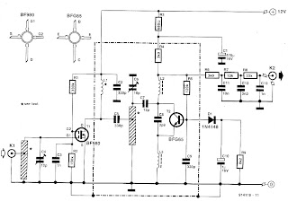
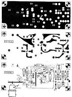
It is a super-regenerative type with an active RF amplifier, T1. The antenna signal is applied to the input inductor via a BNC socket, K1. The input circuit is tuned by trimmer C4. The amplified RF signal is applied to the input of the super-regenerative stage based on transistor T2. Although  the oscillator is, strictly speaking, not tuned, it will lock on to the amplified RF signal applied via coupling capacitor C7. The low-frequency modulation component is extracted from the oscillator signal with the aid of low-pass filter, R6-R7-C12-R8-C13. The signal level at the demodulator output is 50 to 800 mVpp, so that further amplification is required·before the signal can be applied to a digital input.   The inductors in the RF amplifier input and output are made from 1 mm dia. silver-plated wire. The length of the pieces of wire is indicated by the component overlay. The wires run at a height of about 3 mm above the board surface. Note that the stator terminal of C4 is bent upwards and soldered direct to the input inductor. The same goes for junction C6-C7, which is soldered ‘in the air‘, directly op to the hot end of the inductor wire. Inductor L1 consists of 12 turns of 0.6-mm dia. enamelled copper wire. Its internal diameter is 3 mm. Each of chokes g and L3 consists of 4 turns of 0.2-mm dia enamelled copper wire through a 3 mm long ferrite bead. Capacitor C8 is a surface-mount technology (SMT) type which is fitted at the solder side of the board, as are the BFG65 and the BFQSO. The type indica- tion printed on the transistors is legible from the component side of the board. As indicated by the dashed lines on the component overlay, the super-regenerative section of the circuit must be screened from the rest. To do this, it is  best to solder a 20 mm high tin plate box on to the PCB as indicated.


For the transmitter circuit :  UHF FM Remote Control Transmitter Circuit

Readmore → UHF FM Remote Control Receiver Circuit