Saturday, 31 December 2016
UHF FM Remote Control Receiver Circuit
The receiver is intended primarily for use with the remote control UHF transmitter described in the preceding article.
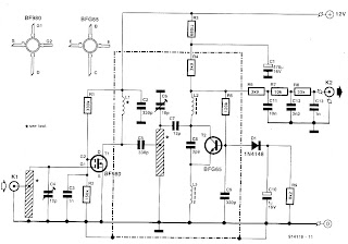
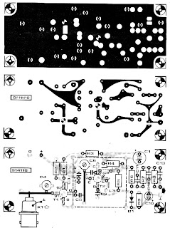
It is a super-regenerative type with an active RF amplifier, T1. The antenna signal is applied to the input inductor via a BNC socket, K1. The input circuit is tuned by trimmer C4. The amplified RF signal is applied to the input of the super-regenerative stage based on transistor T2. Although the oscillator is, strictly speaking, not tuned, it will lock on to the amplified RF signal applied via coupling capacitor C7. The low-frequency modulation component is extracted from the oscillator signal with the aid of low-pass filter, R6-R7-C12-R8-C13. The signal level at the demodulator output is 50 to 800 mVpp, so that further amplification is required·before the signal can be applied to a digital input. The inductors in the RF amplifier input and output are made from 1 mm dia. silver-plated wire. The length of the pieces of wire is indicated by the component overlay. The wires run at a height of about 3 mm above the board surface. Note that the stator terminal of C4 is bent upwards and soldered direct to the input inductor. The same goes for junction C6-C7, which is soldered ‘in the air‘, directly op to the hot end of the inductor wire. Inductor L1 consists of 12 turns of 0.6-mm dia. enamelled copper wire. Its internal diameter is 3 mm. Each of chokes g and L3 consists of 4 turns of 0.2-mm dia enamelled copper wire through a 3 mm long ferrite bead. Capacitor C8 is a surface-mount technology (SMT) type which is fitted at the solder side of the board, as are the BFG65 and the BFQSO. The type indica- tion printed on the transistors is legible from the component side of the board. As indicated by the dashed lines on the component overlay, the super-regenerative section of the circuit must be screened from the rest. To do this, it is best to solder a 20 mm high tin plate box on to the PCB as indicated.


It is a super-regenerative type with an active RF amplifier, T1. The antenna signal is applied to the input inductor via a BNC socket, K1. The input circuit is tuned by trimmer C4. The amplified RF signal is applied to the input of the super-regenerative stage based on transistor T2. Although the oscillator is, strictly speaking, not tuned, it will lock on to the amplified RF signal applied via coupling capacitor C7. The low-frequency modulation component is extracted from the oscillator signal with the aid of low-pass filter, R6-R7-C12-R8-C13. The signal level at the demodulator output is 50 to 800 mVpp, so that further amplification is required·before the signal can be applied to a digital input. The inductors in the RF amplifier input and output are made from 1 mm dia. silver-plated wire. The length of the pieces of wire is indicated by the component overlay. The wires run at a height of about 3 mm above the board surface. Note that the stator terminal of C4 is bent upwards and soldered direct to the input inductor. The same goes for junction C6-C7, which is soldered ‘in the air‘, directly op to the hot end of the inductor wire. Inductor L1 consists of 12 turns of 0.6-mm dia. enamelled copper wire. Its internal diameter is 3 mm. Each of chokes g and L3 consists of 4 turns of 0.2-mm dia enamelled copper wire through a 3 mm long ferrite bead. Capacitor C8 is a surface-mount technology (SMT) type which is fitted at the solder side of the board, as are the BFG65 and the BFQSO. The type indica- tion printed on the transistors is legible from the component side of the board. As indicated by the dashed lines on the component overlay, the super-regenerative section of the circuit must be screened from the rest. To do this, it is best to solder a 20 mm high tin plate box on to the PCB as indicated.


For the transmitter circuit : UHF FM Remote Control Transmitter Circuit
Subscribe to:
Post Comments (Atom)
No comments:
Post a Comment